Tag: TSMC

  • TSMC Boosts 2nm Chip Production and U.S. Expansion Amid AI Race

    TSMC Boosts 2nm Chip Production and U.S. Expansion Amid AI Race

    Key Takeaways

    1. TSMC is set to begin mass production of its 2nm process, N2, in 2025, ahead of its original 2030 timeline.
    2. The company reported a revenue increase of over 40% in Q3 2025, driven by demand for AI technology and high-end smartphones.
    3. TSMC plans to invest $42 billion in expanding its manufacturing capabilities in Taiwan and abroad in 2025.
    4. The Arizona plant is being upgraded for 2nm production, aiming to become a major semiconductor center outside Asia.
    5. TSMC targets to produce around 100,000 wafers per month from its Arizona facility, supporting U.S. efforts for more domestic chip production.


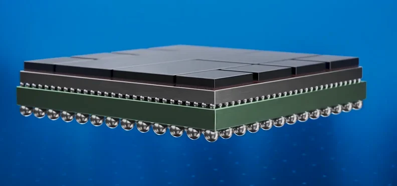
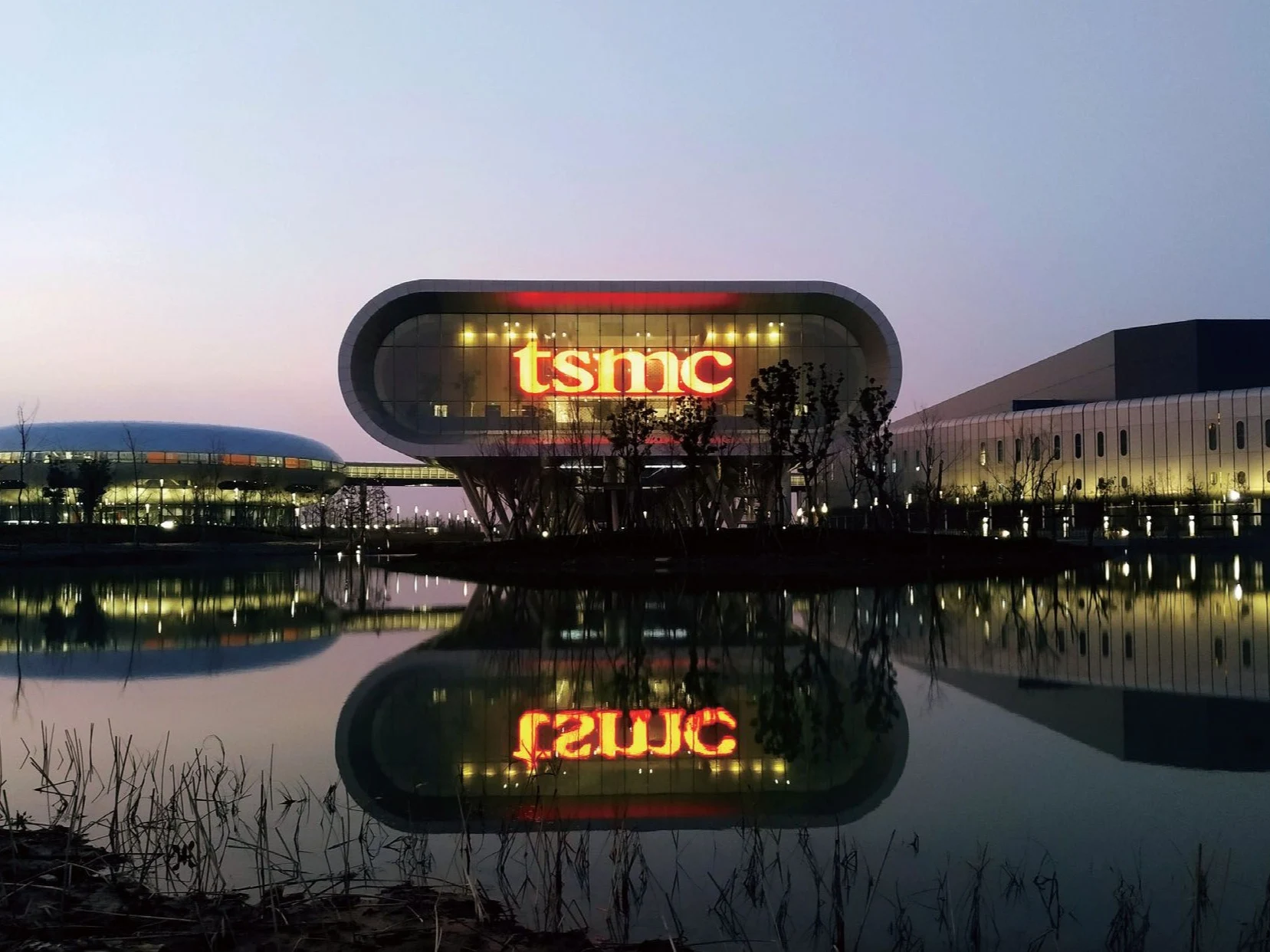
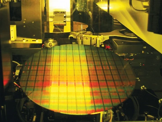
    TSMC is getting ready for the worldwide competition in the semiconductor field. The chip maker has shared that it will begin mass production of its 2nm process, known as N2, sooner than it originally planned.

    Production Timeline Adjustments

    TSMC aims to kick off production of its N2 node in 2025, with a gradual increase in output anticipated for 2026. This change brings the schedule ahead by several years from the initial target of 2030. Executives at the company have indicated that early yields are looking good. They have already commenced work on a better version called N2P, which is set to be released in late 2026.

    Financial Growth Driven by AI

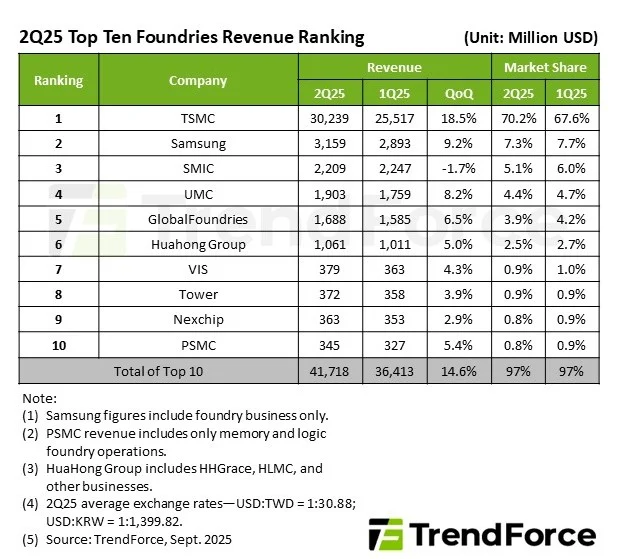
    This accelerated timeline follows TSMC’s impressive Q3 2025 results. The semiconductor giant reported revenues of $33.1 billion, which is more than a 40 percent increase compared to the same time last year. TSMC’s success has been largely fueled by the demand for AI technology and high-end smartphones, with substantial orders coming from clients like Nvidia and Apple.

    Expansion Plans in Manufacturing

    The company is also set to invest heavily in boosting its manufacturing capabilities, both in Taiwan and abroad, with a significant $42 billion allocated for this purpose in 2025.

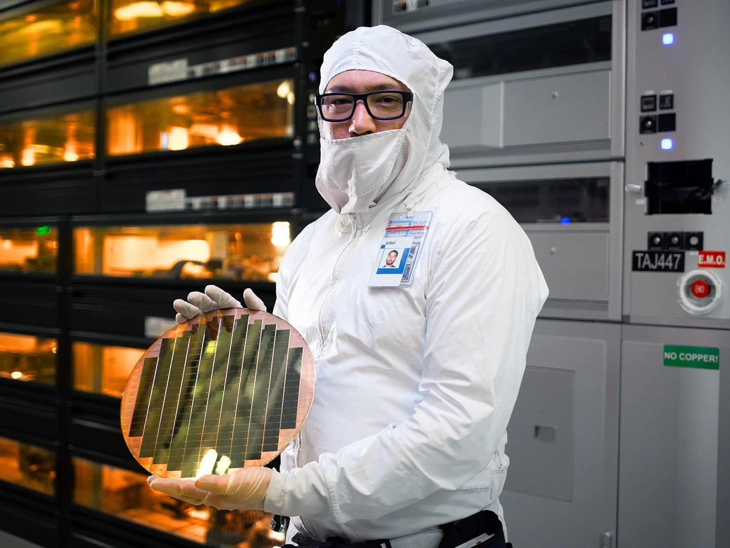
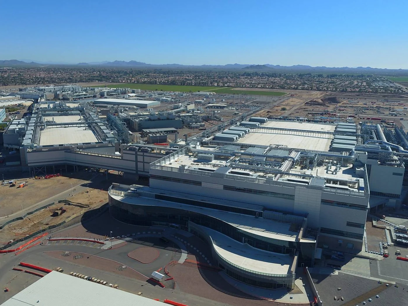
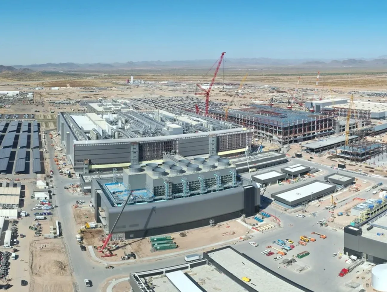
    TSMC has also shared news regarding its Arizona plant. The facility is undergoing upgrades from 3 nm and 4 nm technology to accommodate 2 nm production. This site is expected to be ready for future A16-class manufacturing. TSMC believes this plant could become one of the leading semiconductor centers outside Asia, targeting a 30 percent share of the company’s next-generation output.

    Arizona Production Goals

    The plan is to produce approximately 100,000 wafers each month from the Arizona facility. TSMC is working on establishing the necessary infrastructure for packaging, testing, and suppliers, and is currently exploring options for acquiring additional land. This expansion comes at a crucial time as the United States strives for more domestic chip production and aims to lessen its dependence on foreign manufacturers.

    The competition remains fierce in the global AI and national security arena, but TSMC is positioning itself to lead the charge in the development of next-generation semiconductors for advanced computing.

    Source:
    Link


  • Snapdragon 8 Elite Gen 5 Price Hints at Higher Flagship Costs

    Snapdragon 8 Elite Gen 5 Price Hints at Higher Flagship Costs

    Key Takeaways

    1. Qualcomm has a history of increasing prices for its new products, with the Snapdragon 8 Elite Gen 5 potentially reaching $280.
    2. Pricing can vary among OEMs based on agreements and order sizes, with larger orders likely reducing costs.
    3. The price rise for the Snapdragon 8 Elite Gen 5 is partly due to a 24% increase in costs for the N3P node from TSMC.
    4. Future Snapdragon chips, like the 8 Elite Gen 6, are expected to exceed $300, impacting flagship smartphone pricing.
    5. Samsung is producing 2 nm SoCs for Qualcomm, which could provide a cost-effective alternative to TSMC’s wafers if prices rise further.


    Qualcomm has a history of raising the prices for its newest products. The previous Snapdragon 8 Elite, for instance, was at least 10% higher in cost compared to the 8 Gen 3 for manufacturers. The newly launched Snapdragon 8 Elite Gen 5 is said to potentially reach up to $280.

    Pricing Variations

    This unit price comes from industry predictions, and it’s important to understand that the costs can differ among OEMs based on their agreements with Qualcomm. Additionally, the order sizes can impact the price per unit, with larger orders likely reducing costs. However, this estimate does not take into account the royalty fees that may apply.

    Trends in Pricing

    What’s more significant is the increasing trend in prices for Qualcomm’s flagship SoCs. The price increase for the Snapdragon 8 Elite Gen 5 can’t be solely blamed on Qualcomm, as the chip manufacturer has allegedly paid 24% more for the N3P node from TSMC. Reports indicated that wafer prices rose well before any official announcements were made.

    Future Expectations

    Given this upward trend, it’s reasonable to expect that the upcoming Snapdragon 8 Elite Gen 6 will exceed $300 in price. Such a steep price would inevitably cause flagship smartphones to become even more expensive, making it challenging for manufacturers to offer budget-friendly flagship options (like the OnePlus 13T priced at $509.38 on TradingShenzhen).

    On a positive note, Samsung is said to have started producing 2 nm SoCs for Qualcomm, with early samples reported as sent for testing. If all goes well, this could provide Qualcomm with a viable alternative if TSMC’s 2 nm wafers become unreasonably expensive.

    @yabhishekhd on X

    Source:
    Link


  • Sam Altman Supports TSMC’s Dominance in AI Chip Production

    Sam Altman Supports TSMC’s Dominance in AI Chip Production

    Key Takeaways

    1. Sam Altman prefers TSMC to increase chip production capacity over relying on Intel’s foundry efforts.
    2. TSMC leads in advanced process nodes essential for high-performance AI accelerators, making it the quickest option for chip production.
    3. There are geopolitical concerns regarding TSMC’s Taiwan-based production, prompting calls for a more diversified supply chain.
    4. The demand for modern AI models requires substantial chip capacity; delays could hinder product launches and innovation cycles.
    5. While Intel aims for resilience and localization in its foundry goals, it faces challenges in catching up to TSMC’s capabilities.


    OpenAI’s CEO Sam Altman has a clear message for those in the chip industry: he prefers TSMC to increase its production capacity rather than relying on Intel’s foundry efforts. Altman stated, “I would like TSMC to just build more capacity,” during a recent interview with Stratechery, emphasizing how the urgency from buyers is transforming supply chain priorities.

    Simple Reasoning Behind the Demand

    The reason behind this is pretty simple: TSMC is currently ahead in the advanced process nodes that high-performance AI accelerators require; their factories and yield maturity make them the fastest route for producing more chips. While Intel has been promoting onshoring and its own foundry plans (which includes the 18A node), increasing competitive capacity and achieving reliable yields takes time—time that many AI companies don’t have as their model sizes and computing needs grow. Altman’s public appeal acts as a market signal: when major buyers request more wafers, suppliers and policymakers usually pay attention.

    Geopolitical Considerations

    There’s also a geopolitical aspect to consider. TSMC’s production is primarily located in Taiwan, and although this setup provides buyers quick access to state-of-the-art silicon, it raises strategic and resilience issues for governments and businesses that prefer a more diversified supply chain.

    Sam Altman’s statement can thus be interpreted in two ways: a practical short-term push for immediate capacity, and a subtle acknowledgment that diversification (including onshore alternatives) will take longer to achieve. Reuters reported on Altman’s regional discussions, framing this as part of a broader industry rush for chip capacity and investment.

    Importance for Product Development

    The significance of this lies in the fact that training and deploying modern large models necessitates vast amounts of accelerators made on the latest nodes. If foundry capacity falls behind, companies may encounter delayed launches, increased cloud expenses, and hindered innovation cycles. OpenAI’s public push for TSMC to expand isn’t so much an endorsement of monopoly, but rather a practical request for increased output. This will likely lead to more private deals, increased investor interest, and heightened governmental focus on wafer supply.

    Intel is still a vital player in the long-term strategy: its foundry goals are aimed at resilience, localization, and alternative capacity. However, catching up to TSMC at the forefront is a significant challenge. One can expect a mixed response from the industry, where TSMC addresses the immediate high-performance demand, while Intel and other companies work to grow as part of a larger diversification strategy. In summary, Altman’s comment highlights a crucial tension in the current AI landscape: the endless demand for computing power versus the slow, capital-intensive process of chip manufacturing.

    Source:
    Link


  • Huawei 910C to Replace Nvidia AI Chips with TSMC and Samsung Tech

    Huawei 910C to Replace Nvidia AI Chips with TSMC and Samsung Tech

    Key Takeaways

    1. Huawei has allegedly acquired TSMC dies through a shell company, circumventing export controls to produce nearly three million Ascend 910C AI chips.
    2. The Ascend 910C chip aims to replace Nvidia AI chips, manufactured at SMIC, but faces challenges in yield rates with the 7nm process.
    3. Teardowns confirm the presence of TSMC dies in the 910C, despite TSMC halting production and sales to Huawei post-restrictions.
    4. Huawei is set to produce 653,000 Ascend 910C chips but faces difficulties sourcing high-bandwidth memory (HBM), which could hinder future production.
    5. Production challenges, including poor packaging and thermal inefficiencies, may limit the output of the 910C to about one million units by 2026, despite significant government funding for local chip production.


    Huawei has allegedly found a way to acquire TSMC dies despite existing export control measures, enabling the company to produce its self-developed AI accelerators, as revealed by a detailed examination of the 910C chip.

    Ascend 910C: Huawei’s AI Strategy

    The Ascend 910C represents China’s primary effort to substitute Nvidia AI chips. Huawei is manufacturing this chip at SMIC while rapidly expanding its own foundry capabilities for full vertical integration. However, with SMIC facing challenges in achieving satisfactory yields in its 7nm production process, Huawei is said to have sourced TSMC dies through a shell company, successfully dodging export restrictions for nearly three million Ascend chips.

    Teardown Revelations

    Experts in semiconductor teardowns have validated this information, discovering that the 910C chip indeed contains TSMC dies alongside older high-bandwidth memory (HBM) supplied by Samsung and SK Hynix. TSMC, which faced a $1 billion fine due to the leaked dies, was quick to clarify that the recent teardown of the 910C shows it was produced with the same die “examined by this organization in October 2024, not with a newer die or advanced tech.” They also confirmed that the production and sale of chips sent to Huawei were halted after the restrictions came into play.

    Production Outlook

    Currently, Huawei is on track to produce 653,000 Ascend 910C chips using two TSMC dies, and it reportedly has enough TSMC dies available for production until next summer. However, acquiring high-bandwidth memory to go along with these TSMC chips has proven to be far more challenging. The Samsung or SK Hynix memory that China managed to gather before the HBM controls were implemented is outdated and dwindling fast, leading to reports of Huawei bypassing restrictions by removing memory from loosely packaged products specifically for this task.

    Nonetheless, HBM is expected to be the major obstacle for Huawei’s Ascend 910C AI chip production in the future. The 910C delivers about half the performance of the widely-used Nvidia H100 AI chip, which can be found on Amazon for a price comparable to what Huawei reportedly spends to produce the 910C.

    Production Challenges Ahead

    The 910C’s packaging is somewhat poor and susceptible to thermal inefficiencies, and Huawei still needs to manufacture millions of AI chips to meet domestic demand. Due to these bottlenecks involving HBM and dies, it is estimated that only about a million 910C units could be produced by 2026. However, Chinese government loans aimed at enhancing local AI chip and HBM foundries have reached billions, suggesting that production could ramp up swiftly in the near future.

    Source:
    Link


  • Intel Foundry to Manufacture Future AMD Chips for Enhanced Performance

    Intel Foundry to Manufacture Future AMD Chips for Enhanced Performance

    Key Takeaways

    1. Intel’s upcoming 14A process is expected to signal a resurgence for the company despite challenges with its 18A technology.
    2. Qualcomm is stepping back from Intel Foundry, while Apple and Nvidia show interest in the 14A development.
    3. AMD is monitoring Intel’s progress, which may help maintain a favorable relationship with the current administration and avoid potential tariffs.
    4. Any partnership between Intel and AMD is unlikely to impact AMD’s reliance on TSMC for its advanced products.
    5. Intel’s 14A technology may offer new opportunities, but its competitiveness against TSMC’s offerings remains uncertain.


    Despite facing challenges with its 18A technology, Intel Foundry’s upcoming 14A process is expected to signal a resurgence for the emerging chip manufacturer. Although Qualcomm has chosen to step back, both Apple and Nvidia reportedly show interest in this development. Additionally, if a report from Semafor is to be believed, Intel’s major competitor, AMD, has also taken notice. This move could potentially help AMD maintain a favorable relationship with the current administration and possibly avoid some upcoming tariffs from President Trump.

    Collaboration Possibilities

    Even if a partnership between Intel and AMD comes to fruition, it is improbable that Team Red will rely on Intel Foundry for its most advanced products. AMD’s Epyc Venice CPUs have already been designed using TSMC’s N2 process, with Zen 6 projected to follow next year. Furthermore, Intel’s 14A technology is not expected to begin risk production until 2027, and if Intel continues to experience difficulties, it is likely that this timeline will be delayed. As a result, AMD will probably keep sourcing its main components, like CPU and GPU tiles, from TSMC, while possibly using Intel Foundry for ancillary parts such as Infinity Fabric and I/O dies.

    Future Implications

    In conclusion, while AMD’s interest in Intel Foundry might indicate a strategic move, the practical use of this collaboration appears limited. The ongoing reliance on TSMC for primary hardware components ensures that AMD’s cutting-edge advancements will remain on their current path. Intel’s 14A node may offer new opportunities, but whether it can compete with TSMC’s offerings remains to be seen. Overall, the landscape of chip manufacturing continues to evolve, with various players making moves in a complex arena.

    Source:
    Link


  • Intel 14A Node Cost Higher Than 18A Due to High-NA EUV

    Intel 14A Node Cost Higher Than 18A Due to High-NA EUV

    Key Takeaways

    1. The new 14A node from Intel will be more expensive than the existing 18A node due to advanced High-NA EUV lithography tools costing around $380 million.
    2. The 14A node is expected to improve performance-per-watt by 15-20% and reduce power consumption by 25-35%, featuring new technologies like RibbonFET 2 transistors and Turbo Cells.
    3. Intel’s success with the 14A node relies on attracting external foundry clients; insufficient interest could lead to a slowdown or halt in development.
    4. Intel plans to maintain its partnership with TSMC, with 70% of production in-house and 30% outsourced, and TSMC will manufacture key chip series for Intel.
    5. Intel has secured significant investments, totaling over $7 billion, and anticipates critical developments in 2026 related to the 14A node.


    Intel CFO David Zinsner has recently stated that the new 14A node from Intel will be pricier than the existing 18A node. The increased costs stem from the next-gen High-NA EUV lithography tools, which are priced at around $380 million, in contrast to the $235 million tools currently in use. Importantly, the 14A node is Intel’s first fabrication process tailored specifically for both internal and external foundry clients.

    Performance and Efficiency Boost

    The 14A node is anticipated to deliver roughly 15 to 20 percent improved performance-per-watt when compared to the existing 18A node, along with a power consumption reduction of 25 to 35 percent. This new node incorporates RibbonFET 2 transistors, PowerDirect backside power delivery, and Turbo Cells. Furthermore, the new High-NA EUV tool boasts a much finer resolution of 8nm in a single exposure, a significant improvement over the 13.5nm resolution of the current tools.

    Dependency on External Customers

    Intel must attract external foundry clients to validate the development expenses of the 14A node. If the foundry fails to secure a sufficient number of external customers, the company might need to slow down or possibly halt the node’s development. Nevertheless, CEO Lip-Bu Tan has expressed growing confidence due to enhancements in 18A yield. Additionally, due to US government contract stipulations (which require 51 percent control), Intel Foundry cannot be separated off.

    Ongoing Partnership with TSMC

    On another note, Intel’s CFO claims that the company will likely continue its partnership with TSMC indefinitely. Currently, production is split with 70 percent in-house and 30 percent outsourced to external foundries. It is reported that TSMC is responsible for manufacturing the entire Lunar Lake series and most Arrow Lake chips. Furthermore, Intel is expected to be one of TSMC’s initial clients for 2nm chips, with TSMC set to produce the upcoming Nova Lake chips.

    Recently, Intel has attracted substantial investments, including $2 billion from SoftBank and $5.7 billion from government funding. Additional funding is also anticipated from Mobileye ($1 billion) and Altera ($3.5 billion). Panther Lake on 18A is expected to commence production later this year, with 2026 seen as a crucial year for assessing the progress of the 14A node.

    Source:
    Link


  • Amkor Moves $2B Chip Plant to Peoria for U.S. Semiconductor Security

    Amkor Moves $2B Chip Plant to Peoria for U.S. Semiconductor Security

    Key Takeaways

    1. Amkor is establishing a new advanced packaging and testing facility on a 104-acre site in Peoria, Arizona, with construction starting soon and production expected by early 2028.
    2. The investment for the facility is projected to be $2 billion, creating approximately 2,000 jobs and enhancing the U.S. semiconductor supply chain.
    3. The new site aims to alleviate semiconductor supply chain issues by focusing on high-performance packaging and reducing reliance on Taiwan and South Korea.
    4. The project is backed by $407 million from the CHIPS Act, but a national shortage of semiconductor talent may pose challenges for staffing.
    5. Despite the new facility, immediate solutions for AI server shortages will not be realized until after it becomes operational in 2028, with ongoing reliance on Asian facilities for packaging capacity in the interim.


    Amkor has updated the location for its new advanced packaging and testing facility to a 104-acre site in the Peoria Innovation Core, located in northern Peoria, Arizona. Recently, on August 29, the Peoria City Council approved the land exchange, which replaces the earlier planned 56-acre Vistancia site. Construction is expected to commence shortly, with production scheduled to kick off in early 2028. The company estimates that the investment will reach $2 billion and will generate around 2,000 jobs.

    A Significant Step Forward

    City officials describe this move as a “historic milestone” that will enhance the U.S. semiconductor supply chain. Amkor mentions that the larger space provides greater flexibility to meet the rising demand from customers. Having been active in the Greater Phoenix area since 1984, the company intends to cater to clients in the computing, automotive, and communications sectors from this new facility.

    Addressing Supply Chain Challenges

    The new facility is designed to tackle existing problems within the semiconductor supply chain. Currently, assembly, testing, and packaging are heavily concentrated in Taiwan and South Korea, leading to bottlenecks that have hindered the production of AI chips, like the Nvidia H100. The Peoria site will focus on high-performance packaging platforms, including TSMC’s CoWoS and InFO, which are utilized in data-center GPUs, and possibly Apple silicon, although this remains unconfirmed. TSMC has signed an agreement to send packaging from its Phoenix fabs to Amkor, which will help reduce turnaround times.

    Funding and Labor Challenges

    This project is supported by $407 million from the CHIPS Act along with federal tax incentives, making it one of the most ambitious outsourced packaging projects on American soil, aimed at keeping the U.S. competitive in multi-die systems. Nevertheless, the national shortage of semiconductor talent, estimated at around 70,000 to 90,000 workers, could create challenges for the new plant since automation alone won’t bridge the gap entirely. Amkor plans to collaborate with TSMC and other local Arizona entities to develop a supportive ecosystem.

    Looking Ahead

    However, don’t expect immediate solutions for AI server shortages. For the next few years, packaging capacity will still depend on Asian facilities, with the impact of the U.S. facility only beginning once Peoria starts operations in early 2028. Important milestones to keep an eye on include groundbreaking ceremonies, initial construction developments, installation of tools, hiring and training processes, localizing suppliers, and meeting initial capacity goals.

    Source:
    Link


  • TSMC Nanjing Fab to Lose U.S. Export License Waiver by 2025

    TSMC Nanjing Fab to Lose U.S. Export License Waiver by 2025

    Key Takeaways

    1. The U.S. will revoke TSMC’s Validated End User (VEU) status for its Nanjing factory starting December 31, 2025, requiring individual licensing for shipments.
    2. This change may lead to delays in production, as suppliers must apply for U.S. licenses for tools and materials, with a “presumption of denial” increasing the risk of further delays.
    3. TSMC’s Nanjing facility contributes about 3% of its overall capacity and primarily produces older-generation chips, which could be disrupted by the loss of VEU status.
    4. The U.S. is tightening export controls by revoking VEU status for companies like Samsung and SK Hynix, reflecting a broader strategy to close export control loopholes.
    5. TSMC may face challenges in replacing advanced equipment and requalifying processes at the Nanjing fab, potentially impacting production yields and speed.


    Washington has decided to take away TSMC’s Validated End User (VEU) status for its factory in Nanjing, starting December 31, 2025. This change means that U.S.-controlled shipments to the Chinese facility will no longer have blanket approvals. TSMC has announced that they are “evaluating the situation” and are currently discussing matters with the U.S. government. The goal for TSMC is to keep operations at the Nanjing fab running smoothly without any interruptions. It’s worth mentioning that this represents a change in policy that tightens regulations, not an immediate closure.

    Impact on Supply Chain

    Without the VEU status, suppliers will now need to apply for individual U.S. licenses for tools, spare parts, and specific chemicals that are headed to Nanjing. This could lead to possible delays in production. The decision-making process might come with a “presumption of denial,” which raises the risk of further delays if approvals are not received on time. Previous revocations for companies like Samsung and SK Hynix have resulted in about 1,000 license requests each year. Although TSMC’s situation was not listed in the Federal Register, the outcome remains the same: there will be an increased need for licensing.

    Nanjing Fab Details

    According to Taiwan’s MOEA, TSMC’s Nanjing facility accounts for roughly three percent of the company’s overall capacity. Production at this site began in 2018 and contributed a minor portion of revenue in the past year. The nodes affected include 16-nanometer/12-nanometer FinFET and 28-nanometer-class logic, with the latter being older but still relevant when shipped from U.S.-controlled suppliers. While the Nanjing fab still produces older-generation chips, it depends on advanced equipment for etching, deposition, metrology, and lithography, and losing VEU status could disrupt its operations.

    Similar Moves by the U.S.

    This action is similar to the U.S. revoking VEU status for Samsung and SK Hynix’s facilities in China, which is part of Washington’s strategy to close “export control loopholes.” Although TSMC has a smaller presence in China compared to Samsung or SK Hynix, the impact on the company is likely to be less severe. However, the timing of license approvals still creates uncertainty.

    It seems improbable that TSMC would be able to swap its tools for equipment manufactured in China, especially for lithography needs. Even if they manage to find replacements, the Nanjing fab would have to requalify its processes, which could influence production yields and speed. Should production slow down, Chinese foundries like SMIC and Hua Hong might be able to take over some orders, assuming they have enough capacity to do so.

    Source:
    Link


  • Global Foundry Revenue Hits $41.7B in Q2 2025, TSMC at 70% Share

    Global Foundry Revenue Hits $41.7B in Q2 2025, TSMC at 70% Share

    Key Takeaways

    1. Global foundry earnings reached a record $41.7 billion in Q2 2025, a 14.6% increase quarter-on-quarter.
    2. TSMC led the market with $30.24 billion in revenue, capturing a 70.2% market share, the highest ever for the company.
    3. Demand growth was driven by China’s consumer subsidies and upcoming product launches in smartphones, PCs, and servers.
    4. Tier-2 foundries also grew, with HuaHong Group earning $1.06 billion and other smaller foundries seeing significant increases.
    5. Challenges remain for advanced node production, particularly for SMIC, which faced a 1.7% revenue decline due to shipment delays.


    Global foundry earnings reached an all-time high of $41.7 billion in the second quarter of 2025, marking an increase of 14.6 percent quarter-on-quarter, as reported by TrendForce. TSMC topped the list with an impressive revenue of $30.24 billion, capturing a 70.2 percent share, which is the highest it has ever achieved. Samsung claimed the second spot with $3.16 billion and a 7.3 percent market share, while China’s SMIC secured third place, earning $2.21 billion and holding a market share of 5.1 percent.

    Demand Surge

    The rise in demand was fueled by China’s consumer subsidy initiative and the anticipation of product launches in the latter half of the year for smartphones, notebooks/PCs, and servers. TrendForce predicts that seasonal product trends will continue to drive orders in Q3: advanced nodes are set to gain from flagship chip sales, while mature nodes will benefit from demand for peripheral ICs, with growth expected to slow down from the rapid increase seen in Q2.

    TSMC’s Dominance

    TSMC’s strong position is attributed to its advanced nodes and the scale of its packaging capabilities. Currently, around three-quarters of its revenue is generated from 7nm technology and smaller nodes, with about a quarter coming from 3nm, which is largely driven by Nvidia’s Blackwell GPUs, AMD’s Zen 5 CPUs, and Apple’s M-series Macs. The ramp-up in high-performance chip production and mobile device manufacturing, along with the capacity for advanced packaging, has kept both shipments and average selling prices on the rise.

    Samsung’s foundry revenue increased by 9.2 percent quarter-on-quarter to $3.16 billion, still placing it far behind TSMC. In contrast, SMIC experienced a decline of 1.7 percent due to challenges in advanced node production, as shipment delays affected average selling prices. UMC’s revenue grew by 8.2 percent to $1.9 billion, capturing a 4.4 percent share, while GlobalFoundries saw a 6.5 percent increase to $1.69 billion, holding a 3.9 percent share. Despite substantial investments, Intel Foundry’s revenue continues to be significantly lower.

    Growth Among Tier-2 Foundries

    Tier-2 foundries also saw growth thanks to orders for peripheral ICs: HuaHong Group reached approximately $1.06 billion, accounting for 2.5 percent of the market, Vanguard earned $379 million, Tower made $372 million, Nexchip reached $363 million, and PSMC garnered $345 million. While supply is anticipated to improve this year, costs are expected to stay high. The TSMC 2nm node is likely to come with a higher price tag, as GPU manufacturers are already raising prices to counterbalance wafer costs.

    Source:
    Link


  • TSMC Speeds Up 1.4nm Process as Intel and Samsung Adjust Plans

    TSMC Speeds Up 1.4nm Process as Intel and Samsung Adjust Plans

    Key Takeaways

    1. TSMC is advancing quickly in semiconductor manufacturing, moving towards 1.4nm production while 2nm chips are not yet widespread.
    2. The company plans to build four new factories, with the first expected to be operational by the end of 2027 and mass production starting in late 2028.
    3. TSMC’s progress comes as competitors Intel and Samsung reassess their manufacturing plans, with Intel potentially halting its 1.4nm development and Samsung delaying its targets to 2029.
    4. The current market is primarily using 3nm technology, with TSMC’s 3nm process being utilized in various CPUs from Intel and Apple.
    5. New semiconductor nodes typically debut in mobile chips, with the upcoming Galaxy S26 series set to use the 2nm process for its Exynos 2600 CPU.


    The race in semiconductor manufacturing is moving swiftly, and TSMC, the leading company in this field, is eager to further solidify its dominance. Although 2nm chips haven’t seen widespread use yet, it appears that TSMC is already pushing ahead with its 1.4nm production process. New factories dedicated to this advanced technology might be established as soon as next year, with plans for mass production to commence the following year.

    Breakthrough in Manufacturing

    According to UDN (translated by machines), TSMC has achieved a significant advancement in its 1.4nm production, enabling a quicker ramp-up of output, which begins with the construction of new factories. The company is set to build four facilities, with the first expected to be operational by the end of 2027 after its risk trial production is completed. This indicates that mass production could kick off in the latter half of 2028. TSMC has also reportedly notified its suppliers to get ready with the essential equipment for the 1.4nm production setup.

    Production Phases and Future Plans

    Among the four factories in the plans, two will initiate mass production of the new node in 2028 as part of the initial phase. In the second phase, the other two factories could potentially be utilized for an even more advanced 1nm manufacturing process.

    This significant progress for TSMC arrives at a moment when rivals like Intel and Samsung are reevaluating their manufacturing roadmaps. Intel is considering halting its A14, the 1.4nm process development, while Samsung has delayed its 1.4nm targets to 2029 to improve yields with their 2nm process.

    Current Market Landscape

    However, the existing PC market is still primarily operating on the 3nm manufacturing process, with 2nm technology still absent. Intel’s Arrow Lake and Lunar Lake CPUs utilize TSMC’s 3nm process, whereas Apple’s latest M4 platform is built on TSMC’s N3E process, which is the second generation of 3nm. Generally, new nodes are first implemented in mobile chips before they reach mainstream desktop computing. The Exynos 2600, set to power the upcoming Galaxy S26 series, will be the first mobile CPU utilizing this process. Similarly, while Apple’s soon-to-be-released iPhone 17 series is expected to maintain the 3nm process, the iPhone 18 series equipped with the A20 SoC will likely transition to 2nm technology.

    Source:
    Link