
Key Takeaways
1. Amkor is establishing a new advanced packaging and testing facility on a 104-acre site in Peoria, Arizona, with construction starting soon and production expected by early 2028.
2. The investment for the facility is projected to be $2 billion, creating approximately 2,000 jobs and enhancing the U.S. semiconductor supply chain.
3. The new site aims to alleviate semiconductor supply chain issues by focusing on high-performance packaging and reducing reliance on Taiwan and South Korea.
4. The project is backed by $407 million from the CHIPS Act, but a national shortage of semiconductor talent may pose challenges for staffing.
5. Despite the new facility, immediate solutions for AI server shortages will not be realized until after it becomes operational in 2028, with ongoing reliance on Asian facilities for packaging capacity in the interim.
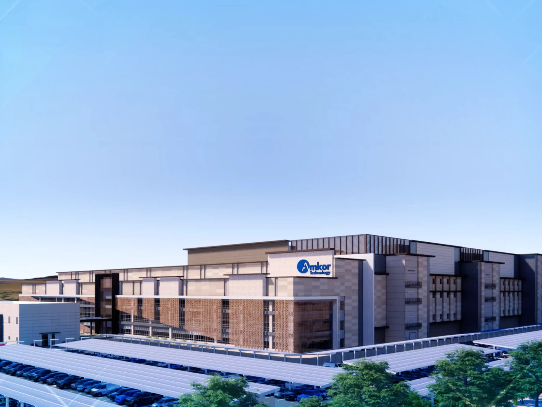
Amkor has updated the location for its new advanced packaging and testing facility to a 104-acre site in the Peoria Innovation Core, located in northern Peoria, Arizona. Recently, on August 29, the Peoria City Council approved the land exchange, which replaces the earlier planned 56-acre Vistancia site. Construction is expected to commence shortly, with production scheduled to kick off in early 2028. The company estimates that the investment will reach $2 billion and will generate around 2,000 jobs.
A Significant Step Forward
City officials describe this move as a “historic milestone” that will enhance the U.S. semiconductor supply chain. Amkor mentions that the larger space provides greater flexibility to meet the rising demand from customers. Having been active in the Greater Phoenix area since 1984, the company intends to cater to clients in the computing, automotive, and communications sectors from this new facility.
Addressing Supply Chain Challenges
The new facility is designed to tackle existing problems within the semiconductor supply chain. Currently, assembly, testing, and packaging are heavily concentrated in Taiwan and South Korea, leading to bottlenecks that have hindered the production of AI chips, like the Nvidia H100. The Peoria site will focus on high-performance packaging platforms, including TSMC’s CoWoS and InFO, which are utilized in data-center GPUs, and possibly Apple silicon, although this remains unconfirmed. TSMC has signed an agreement to send packaging from its Phoenix fabs to Amkor, which will help reduce turnaround times.
Funding and Labor Challenges
This project is supported by $407 million from the CHIPS Act along with federal tax incentives, making it one of the most ambitious outsourced packaging projects on American soil, aimed at keeping the U.S. competitive in multi-die systems. Nevertheless, the national shortage of semiconductor talent, estimated at around 70,000 to 90,000 workers, could create challenges for the new plant since automation alone won’t bridge the gap entirely. Amkor plans to collaborate with TSMC and other local Arizona entities to develop a supportive ecosystem.
Looking Ahead
However, don’t expect immediate solutions for AI server shortages. For the next few years, packaging capacity will still depend on Asian facilities, with the impact of the U.S. facility only beginning once Peoria starts operations in early 2028. Important milestones to keep an eye on include groundbreaking ceremonies, initial construction developments, installation of tools, hiring and training processes, localizing suppliers, and meeting initial capacity goals.
Source:
Link
Leave a Reply