Tag: high-NA EUV

  • Intel 14A Node Cost Higher Than 18A Due to High-NA EUV

    Intel 14A Node Cost Higher Than 18A Due to High-NA EUV

    Key Takeaways

    1. The new 14A node from Intel will be more expensive than the existing 18A node due to advanced High-NA EUV lithography tools costing around $380 million.
    2. The 14A node is expected to improve performance-per-watt by 15-20% and reduce power consumption by 25-35%, featuring new technologies like RibbonFET 2 transistors and Turbo Cells.
    3. Intel’s success with the 14A node relies on attracting external foundry clients; insufficient interest could lead to a slowdown or halt in development.
    4. Intel plans to maintain its partnership with TSMC, with 70% of production in-house and 30% outsourced, and TSMC will manufacture key chip series for Intel.
    5. Intel has secured significant investments, totaling over $7 billion, and anticipates critical developments in 2026 related to the 14A node.


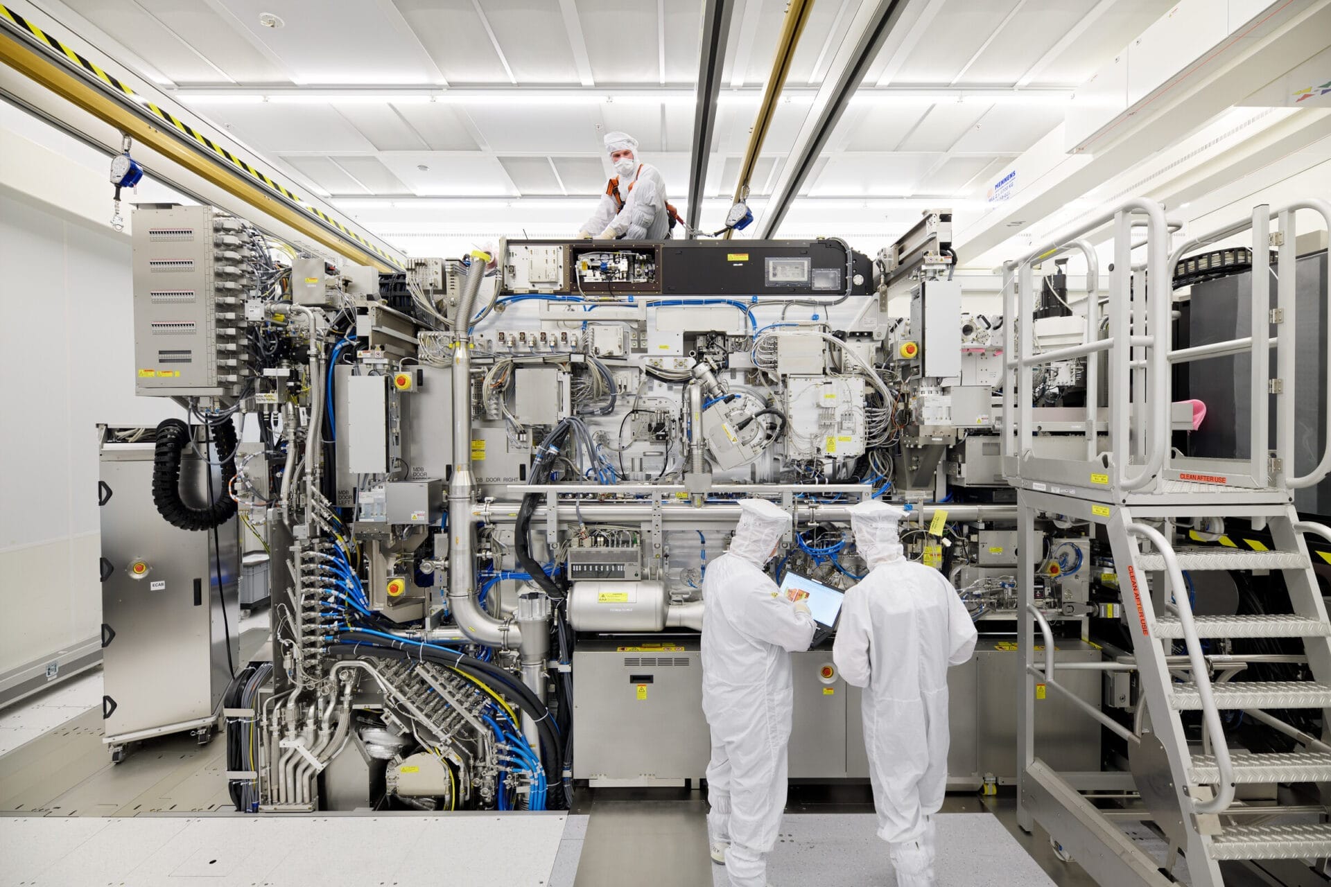
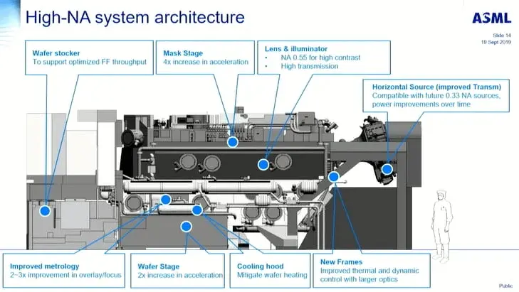
    Intel CFO David Zinsner has recently stated that the new 14A node from Intel will be pricier than the existing 18A node. The increased costs stem from the next-gen High-NA EUV lithography tools, which are priced at around $380 million, in contrast to the $235 million tools currently in use. Importantly, the 14A node is Intel’s first fabrication process tailored specifically for both internal and external foundry clients.

    Performance and Efficiency Boost

    The 14A node is anticipated to deliver roughly 15 to 20 percent improved performance-per-watt when compared to the existing 18A node, along with a power consumption reduction of 25 to 35 percent. This new node incorporates RibbonFET 2 transistors, PowerDirect backside power delivery, and Turbo Cells. Furthermore, the new High-NA EUV tool boasts a much finer resolution of 8nm in a single exposure, a significant improvement over the 13.5nm resolution of the current tools.

    Dependency on External Customers

    Intel must attract external foundry clients to validate the development expenses of the 14A node. If the foundry fails to secure a sufficient number of external customers, the company might need to slow down or possibly halt the node’s development. Nevertheless, CEO Lip-Bu Tan has expressed growing confidence due to enhancements in 18A yield. Additionally, due to US government contract stipulations (which require 51 percent control), Intel Foundry cannot be separated off.

    Ongoing Partnership with TSMC

    On another note, Intel’s CFO claims that the company will likely continue its partnership with TSMC indefinitely. Currently, production is split with 70 percent in-house and 30 percent outsourced to external foundries. It is reported that TSMC is responsible for manufacturing the entire Lunar Lake series and most Arrow Lake chips. Furthermore, Intel is expected to be one of TSMC’s initial clients for 2nm chips, with TSMC set to produce the upcoming Nova Lake chips.

    Recently, Intel has attracted substantial investments, including $2 billion from SoftBank and $5.7 billion from government funding. Additional funding is also anticipated from Mobileye ($1 billion) and Altera ($3.5 billion). Panther Lake on 18A is expected to commence production later this year, with 2026 seen as a crucial year for assessing the progress of the 14A node.

    Source:
    Link


  • SK Hynix Launches First High-NA EUV Lithography Tool at M16 Fab

    SK Hynix Launches First High-NA EUV Lithography Tool at M16 Fab

    Key Takeaways

    1. SK Hynix has successfully installed the first High-NA EUV lithography system for mass production at its M16 facility in South Korea.
    2. The ASML TWINSCAN EXE:5200B system offers 40% greater numerical aperture, enabling smaller features and denser transistor arrangements.
    3. SK Hynix plans to quickly prototype new DRAM structures and streamline EUV processes to enhance competitiveness and reduce costs.
    4. The adoption of High-NA EUV technology positions SK Hynix ahead of competitors like Micron and Samsung in the DRAM market.
    5. This milestone marks a significant step towards next-generation DRAM production and reduces risks associated with future technology transitions.


    SK Hynix has revealed that it has successfully put together the first High-NA EUV lithography system intended for mass production at its M16 facility located in Icheon, South Korea. This achievement was celebrated by executives from both SK Hynix’s research and development and manufacturing divisions, along with ASML’s customer lead for SK Hynix, during a special event on-site. The primary aim of this system is to boost the creation and supply of next-generation DRAM while reinforcing domestic leadership in AI-memory and improving supply-chain reliability through close cooperation with partners. This achievement sets SK Hynix apart from competitors who still depend on Low-NA EUV technology.

    Enhanced Capabilities

    The ASML TWINSCAN EXE:5200B system provides around 40% greater numerical aperture (NA) than its Low-NA alternative, allowing for features that are 1.7 times smaller and approximately 2.9 times denser in terms of transistors in a single exposure. This machine can reach an impressive resolution of 8nm, which is a notable enhancement compared to the existing 13nm resolution found in Low-NA systems. ASML describes this advancement as “opening up a new chapter.”

    Accelerating Development

    In the initial phase, SK Hynix intends to quickly prototype various new DRAM structures, such as capacitor trenches, bitlines, and wordlines, to speed up the development of nodes. The company also aims to streamline its current EUV process flows, which should help in making costs more competitive as the development progresses.

    Future iterations of DRAM are likely to shift to High-NA EUV around the 2030s; thus, this tool mitigates risks associated with that transition early on. Since 2021, SK Hynix has broadened its EUV presence in DRAM, and this milestone signifies the next phase in its journey toward next-gen DRAM production.

    Competitive Edge

    Being among the first to set up High-NA EUV systems at a mass-production site gives SK Hynix an edge over competitors like Micron and Samsung, enhancing its position in the marketplace. Although ASML had previously constructed pre-production High-NA systems (the NXE:5000 series) at Intel’s D1X fab, SK Hynix’s installation represents the inaugural assembly of the new EXE:5200B system at a client fab specifically configured for large-scale production.

    Source:
    Link


  • Samsung Acquires 2nm Chip Tool from ASML: Impact on Exynos 2600?

    Samsung Acquires 2nm Chip Tool from ASML: Impact on Exynos 2600?

    Key Takeaways

    1. Samsung has acquired the first TWINSCAN EXE:5000 High-NA EUV machine from ASML, crucial for producing the 2nm Exynos 2600 chip.
    2. The launch of the Exynos 2500 chip has faced delays due to performance issues and low yield rates from the 3nm process node.
    3. The new High-NA EUV machine could help improve yield rates, allowing for the use of the Exynos 2600 in future Galaxy flagship models.
    4. Samsung’s investment in this technology may reduce reliance on Qualcomm chips and lower manufacturing costs.
    5. Upcoming Galaxy S25 models are expected to resemble their predecessors, with notable differences only in the Ultra model’s design.


    The recent buzz revolves around Samsung’s purchase of High-NA EUV machinery from ASML, which is the only company that makes such equipment. Earlier this month, the first TWINSCAN EXE:5000 High-NA EUV machine was delivered to Samsung’s Hwaseong Campus in South Korea. This machine is said to be essential for producing the 2nm Exynos 2600 chip.

    Potential Impact on Exynos 2600

    Samsung faced challenges in launching the Exynos 2500 chip on time, which was expected to power the base and plus variants of the Galaxy S25 series. There have been whispers about this chip being used in upcoming foldable devices, but nothing is confirmed at this moment.

    The delay is largely linked to the performance issues of the Exynos 2500, which reportedly does not align with the standards that Samsung’s mobile division has established for flagship and foldable models. A significant factor causing the hold-up with the Exynos 2500 was the yield rate of the 3nm process node, which measures the proportion of functional chips produced compared to the total made.

    Improvements on the Horizon

    With the arrival of the advanced High-NA EUV machine, Samsung Foundry may be able to resolve these yield problems. This could pave the way for utilizing the Exynos 2600 in future Galaxy flagship models, particularly the base and plus versions, similar to previous launches. Considering the enhancements seen with the Exynos 2200 and Exynos 2400, it appears Samsung Foundry is making progress.

    While this investment requires some upfront costs, lowering manufacturing expenses (due to reduced reliance on Qualcomm chips) might motivate the company to channel resources into redesigning and upgrading their hardware. After all, the Galaxy S25 and S25 Plus are essentially similar to their predecessors, with the Ultra model only standing out in hardware by its rounded edges and flat middle frame.

    Source:
    Link


  • TSMC Invests $350M in High NA EUV for 1.4nm Chip Tech

    TSMC Invests $350M in High NA EUV for 1.4nm Chip Tech

    Taiwan Semiconductor Manufacturing Corporation (TSMC) is planning to buy ASML’s newest High NA EUV lithography system by the end of 2024. This is a big step for the semiconductor field. The machine, called the Twinscan EXE:5000, costs around $350 million and is filled with state-of-the-art tech for chip production.

    Advanced Technology Features

    This high-tech system has an incredible 8nm resolution and operates with a 13.5nm EUV light wavelength. It allows chipmakers to create smaller chips and fit in up to 2.9 times more transistors than what was possible before. TSMC aims to implement this technology in its upcoming 1.4nm (A14) manufacturing process, intending to start mass production by 2027.

    Industry Adoption

    Intel has already taken the leap by being the first to use High NA EUV, having set up two machines at its facility in Oregon earlier in 2024. Samsung is expected to follow suit, likely by early 2025. Currently, Intel, Samsung, and TSMC are the only confirmed companies with access to ASML’s advanced technology, primarily due to international trade regulations that prevent Chinese companies from obtaining it.

    Challenges Ahead

    Although ASML has claimed to receive 10-20 orders for these machines, bringing them into operation isn’t as easy as it sounds. Their large size means that manufacturers may have to significantly upgrade their existing facilities or even construct new ones. Additionally, these machines have a smaller imaging field compared to current NA EUV systems, which requires a redesign of chip architectures.

    TSMC’s decision to invest in High NA EUV highlights its dedication to leading in advanced chip manufacturing, especially as the demand for AI chips keeps rising. Even though it might take a few years before mass production with this technology truly begins, it represents a move towards the future of semiconductor manufacturing.

  • TSMC to Receive $380M ASML High-NA EUV Lithography Machines

    TSMC to Receive $380M ASML High-NA EUV Lithography Machines

    ASML (Advanced Semiconductor Materials Lithography) is a Dutch company that specializes in the design and manufacturing of lithography machines for the semiconductor sector. These machines play a crucial role in the chip-making process.

    Access to ASML’s state-of-the-art lithography technology has significantly contributed to TSMC’s (Taiwan Semiconductor Manufacturing Company) success as a leading contract chip manufacturer, serving major industry players like NVIDIA and Qualcomm.

    High-NA Lithography Technology

    ASML’s latest announcement reveals that it will ship its most advanced lithography machine, valued at US$ 380 million (~2.753 billion yuan), to TSMC within this year. ASML’s Chief Financial Officer, Roger Dassen, disclosed during a recent conference call that both TSMC and Intel, their two biggest clients, will receive the high numerical aperture (high-NA) extreme ultraviolet (EUV) lithography technology by 2024.

    ASML has already delivered the world’s first commercial high-NA EUV lithography machine to Intel, with the initial unit being sent to an Oregon factory in late December. The exact timing for TSMC to receive this advanced tool remains unspecified.

    The high-NA lithography technology is anticipated to shrink transistor sizes by 66%. This reduction enables chip manufacturers to pack more transistors into the same silicon area, enhancing power efficiency and sustained performance.

    Technical Advancements

    The high-NA EUV system achieves a numerical aperture of 0.55, improving accuracy and allowing for more intricate silicon patterning compared to previous EUV systems with a 0.33 numerical aperture lens. The new machine is also 30% larger than its predecessors, which already required three Boeing 747s for transportation.

    Regarding TSMC, the development of their 2nm nodes is reportedly on track. The company plans to start developing the N3X and N2 processes in Q2 2025, with mass production of N2P and A16 slated for Q2 2026. The 2nm process will incorporate Gate-all-around FETs (GAAFET).

    TSMC predicts that its 2nm process will offer a 10% to 15% performance boost and reduce power consumption by 25% to 30%.


    TSMC to Receive 0M ASML High-NA EUV Lithography Machines