
Key Takeaways
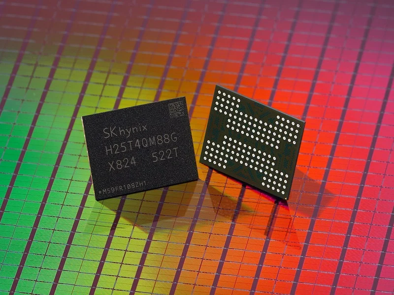
1. SK Hynix has successfully installed the first High-NA EUV lithography system for mass production at its M16 facility in South Korea.
2. The ASML TWINSCAN EXE:5200B system offers 40% greater numerical aperture, enabling smaller features and denser transistor arrangements.
3. SK Hynix plans to quickly prototype new DRAM structures and streamline EUV processes to enhance competitiveness and reduce costs.
4. The adoption of High-NA EUV technology positions SK Hynix ahead of competitors like Micron and Samsung in the DRAM market.
5. This milestone marks a significant step towards next-generation DRAM production and reduces risks associated with future technology transitions.
SK Hynix has revealed that it has successfully put together the first High-NA EUV lithography system intended for mass production at its M16 facility located in Icheon, South Korea. This achievement was celebrated by executives from both SK Hynix’s research and development and manufacturing divisions, along with ASML’s customer lead for SK Hynix, during a special event on-site. The primary aim of this system is to boost the creation and supply of next-generation DRAM while reinforcing domestic leadership in AI-memory and improving supply-chain reliability through close cooperation with partners. This achievement sets SK Hynix apart from competitors who still depend on Low-NA EUV technology.
Enhanced Capabilities
The ASML TWINSCAN EXE:5200B system provides around 40% greater numerical aperture (NA) than its Low-NA alternative, allowing for features that are 1.7 times smaller and approximately 2.9 times denser in terms of transistors in a single exposure. This machine can reach an impressive resolution of 8nm, which is a notable enhancement compared to the existing 13nm resolution found in Low-NA systems. ASML describes this advancement as “opening up a new chapter.”
Accelerating Development
In the initial phase, SK Hynix intends to quickly prototype various new DRAM structures, such as capacitor trenches, bitlines, and wordlines, to speed up the development of nodes. The company also aims to streamline its current EUV process flows, which should help in making costs more competitive as the development progresses.
Future iterations of DRAM are likely to shift to High-NA EUV around the 2030s; thus, this tool mitigates risks associated with that transition early on. Since 2021, SK Hynix has broadened its EUV presence in DRAM, and this milestone signifies the next phase in its journey toward next-gen DRAM production.
Competitive Edge
Being among the first to set up High-NA EUV systems at a mass-production site gives SK Hynix an edge over competitors like Micron and Samsung, enhancing its position in the marketplace. Although ASML had previously constructed pre-production High-NA systems (the NXE:5000 series) at Intel’s D1X fab, SK Hynix’s installation represents the inaugural assembly of the new EXE:5200B system at a client fab specifically configured for large-scale production.
Source:
Link
Leave a Reply