Tag: ASML

  • China Develops Successful Prototype of EUV Machine

    China Develops Successful Prototype of EUV Machine

    Key Takeaways

    1. China has developed an EUV lithography machine in Shenzhen with help from ex-ASML engineers, marking a significant advancement in its chipmaking capabilities.

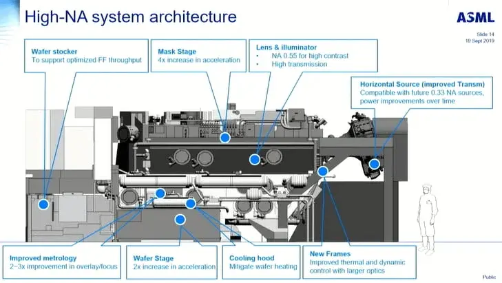
    2. The EUV machine is not yet ready for chip production, with full functionality expected by 2028 or 2030, while competitors may advance to high-NA EUV technology.

    3. China will need to produce the EUV machine’s components domestically and acquire used parts from other vendors due to the lack of official support from ASML.

    4. China has previously relied on older DUV machines to create advanced chips, pushing their limits to produce 5-nm-class chips.

    5. Despite this achievement, China faces major challenges in scaling production and navigating the complexities of new technology.


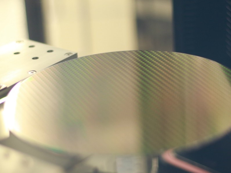
    A recent report from Reuters reveals that China has achieved a major milestone by developing an EUV (Extreme Ultraviolet) lithography machine at a lab in Shenzhen, with help from several ex-ASML engineers. This advancement validates earlier speculations and represents a crucial step forward in China’s chipmaking capabilities. It could enable Chinese firms like SMIC to create advanced chips that could rival those produced by TSMC, Intel, and Samsung. The project was reportedly kept under wraps, with the engineers working using pseudonyms.

    Future Challenges Ahead

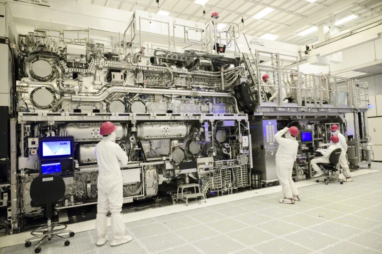
    Despite this progress, the EUV machine still doesn’t have the ability to manufacture chips just yet. It is anticipated to reach full functionality by 2028 or potentially as late as 2030. By that time, industry rivals are expected to have moved on to high-NA EUV, the next-gen lithography technology created by ASML. Furthermore, scaling up production will be a tough task, as China will need to produce everything domestically due to ASML’s absence of official backing. To make matters more complicated, it must also acquire used components from different vendors, including Nikon and Canon.

    Relying on Older Technology

    Up until this point, China has depended on older DUV (Deep Ultraviolet) machines, which are the only models it can legally obtain from ASML. SMIC’s N+3 node has pushed DUV beyond its traditional limits by creating 5-nm-class chips like the Kirin 9030. There was even a recent patent that explored pushing the technology down to 2 nm. However, with the new EUV development, this may not be necessary due to the technology’s complexity and low yield rates.

    In conclusion, this report signifies a notable achievement for China, but significant hurdles remain in the way of fully realizing its chipmaking ambitions.

    Source:
    Link


  • German Engineer Gets 3 Years for Leaking ASML, NXP Tech to Russia

    German Engineer Gets 3 Years for Leaking ASML, NXP Tech to Russia

    Key Takeaways

    1. A German engineer, Aksenov, received a three-year prison sentence for illegally transferring secret semiconductor technology to Russia.
    2. Aksenov copied sensitive design files and documents from ASML and NXP onto external drives, which were found in his home.
    3. The transferred information is believed to have potentially reached the Russian FSB intelligence agency.
    4. ASML and NXP are key targets for espionage due to their valuable intellectual property in electronics.
    5. Aksenov’s claim that he was not spying was rejected by the court, which noted violations of EU sanctions against providing technology to Russia.


    A Rotterdam court has given a three-year prison sentence to German Aksenov, a 43-year-old ex-process engineer who worked at ASML and NXP, for illegally transferring secret semiconductor technology to a contact in Russia.

    Details of the Case

    Investigators discovered that Aksenov had copied design files and production-line documents from his company’s servers onto USB drives and external hard drives, which were later found in his home. He also shared manufacturing information with a Russian associate, and prosecutors suspect that these materials eventually made their way to the FSB intelligence agency.

    Importance of the Companies

    ASML, the only provider of extreme-ultraviolet lithography equipment crucial for modern chip-making, along with NXP, known for co-developing near-field communication technology, are major targets for spying due to the significant value of their intellectual property in both civilian and military electronics. Even though prosecutors asked for a four-year sentence, the court decided on a shorter term after finding no proof that Aksenov received payment for the information.

    Court Proceedings

    During previous hearings, Aksenov acknowledged having company files but insisted he wasn’t spying, claiming they were meant to “keep up with professional knowledge.” The court dismissed this claim, emphasizing that the engineer intentionally took restricted materials without considering compliance with sanctions.

    The ruling points out breaches of European Union sanctions that were put in place in 2014, which forbid offering “technical assistance” or restricted technologies to Russian organizations.

    Source:
    Link

  • SiCarrier Seeks $2.8B Funding at $11B Valuation in China

    SiCarrier Seeks $2.8B Funding at $11B Valuation in China

    Key Takeaways

    1. SiCarrier, referred to as the “Chinese ASML,” is seeking $2.8 billion in external fundraising, aiming for an $11 billion valuation to reduce reliance on imported chip-manufacturing equipment.

    2. The Shenzhen local government plans to sell about 25% of a SiCarrier subsidiary, potentially valuing it at 80 billion yuan, with proceeds focused on research and development.

    3. Founded in 2021, SiCarrier specializes in first-generation technology and aims to provide various semiconductor manufacturing tools, showcased at SEMICON China.

    4. Analysts note that many of SiCarrier’s products are still in development and lack the validation needed for semiconductor clients, raising concerns about the speed of monetization.

    5. SiCarrier faces challenges from U.S. export regulations and restrictions, which complicate access to foreign technologies and emphasize China’s push for self-sufficiency in the semiconductor industry.


    Shenzhen’s SiCarrier, often called the “Chinese ASML,” is gearing up for its first round of external fundraising, aiming to gather about $2.8 billion while being valued at around $11 billion. This fundraising initiative is part of a larger strategy by China’s semiconductor industry to reduce dependence on imported chip-manufacturing equipment.

    Sale of Subsidiary Stakes

    Sources close to the situation indicate that the Shenzhen local government plans to sell roughly 25 percent of a SiCarrier subsidiary, which does not possess lithography assets. This sale could value the unit at approximately 80 billion yuan (around $11.1 billion) and might be finalized within a few weeks, potentially becoming one of the largest yuan-denominated fundraising efforts in the country this year. The funds raised will primarily be used for research and development, and several state-owned enterprises along with local venture capitalists have expressed interest.

    Company Background and Goals

    Founded in 2021, SiCarrier operates as a wholly-owned subsidiary of the Shenzhen State-owned Assets Supervision and Administration Commission. The firm focuses on “first-generation technology, materials, and equipment,” with a core team that has over twenty years of experience in electronic equipment engineering. Its public documents outline a product roadmap that includes etching, diffusion, thin-film deposition, and metrology tools, which are aimed at prominent fabs and research institutions in China.

    The extensive product roadmap was showcased at SEMICON China in March, where SiCarrier presented 31 tools categorized into six groups, each named after well-known Chinese mountains. The categories include epitaxial deposition (Emei Series), atomic-layer deposition (Ali Series), physical vapor deposition (Putuo Series), etching (Wuyi Series), chemical vapor deposition (Changbai Series), and various measurement platforms. Domestic analysts praised this reveal as a significant milestone for Chinese chip equipment manufacturers.

    Challenges Ahead

    Despite the excitement, independent assessments suggest that most of the machines introduced are still in the development stage and have not yet undergone the extensive validation that semiconductor clients typically require. Bernstein Research and industry experts warn that constructing and certifying complex wafer-fab machinery generally takes many years, leading to doubts about how swiftly SiCarrier can monetize its product line.

    SiCarrier’s growth ambitions are set against a backdrop of stringent U.S. export regulations. The company was added to an American entity list late last year due to suspected connections with Huawei, which both firms deny. These restrictions have hindered access to foreign technologies and have heightened China’s urgency for self-sufficiency. While it’s still unclear if SiCarrier can expand rapidly enough to compete with established international suppliers, its forthcoming capital raise indicates that China is willing to make significant investments to bridge that gap.

    Source:
    Link

  • ASML CEO: Chinese Chipmakers 10-15 Years Behind Global Leaders

    ASML CEO: Chinese Chipmakers 10-15 Years Behind Global Leaders

    ASML’s chief executive officer, Christophe Fouquet, recently stated that Chinese semiconductor firms such as Huawei and SMIC are still around 10 to 15 years behind leading companies including Intel, TSMC, and Samsung. This assertion comes amid increasing scrutiny of ASML’s relationships with Chinese clients, largely due to rising geopolitical tensions.

    Challenges with EUV Technology

    Fouquet pointed out that a major problem for Chinese manufacturers is their lack of access to cutting-edge extreme ultraviolet (EUV) lithography machines. These machines are essential for keeping pace with the global industry leaders. ASML’s EUV machines, which cost about 400 million euros each, are crucial for producing advanced semiconductors. In fact, transporting the necessary components alone requires seven cargo planes.

    ASML’s Financial Performance

    In spite of these hurdles, the Dutch lithography giant reported impressive figures for the third quarter of 2024, with net sales reaching 7.5 billion euros and profits of 2.1 billion euros. However, new orders dropped to 2.6 billion euros, which is less than half of the 5.6 billion euros seen in the previous quarter. Nevertheless, China continues to represent a significant portion of ASML’s revenue, contributing 47 percent to the company’s Q3 2024 sales.

    Future Sales Predictions

    UBS analysts are forecasting that ASML might experience nearly a 25 percent decrease in its Chinese sales in the coming year, with as much as 45 percent of its total revenue from China at risk if more restrictions are implemented. While the U.S. is urging ASML to halt servicing existing equipment in China, the Netherlands has not yet followed suit with these demands.

    To provide some context, ASML and its partners have invested over twenty years in refining the commercial EUV ecosystem. Although Huawei and its partners are working on developing their own EUV systems, experts believe it could take just as long to establish a comparable ecosystem, even if they gain access to some older technologies that have already been developed.

    Source: Link

  • TSMC to Receive $380M ASML High-NA EUV Lithography Machines

    TSMC to Receive $380M ASML High-NA EUV Lithography Machines

    ASML (Advanced Semiconductor Materials Lithography) is a Dutch company that specializes in the design and manufacturing of lithography machines for the semiconductor sector. These machines play a crucial role in the chip-making process.

    Access to ASML’s state-of-the-art lithography technology has significantly contributed to TSMC’s (Taiwan Semiconductor Manufacturing Company) success as a leading contract chip manufacturer, serving major industry players like NVIDIA and Qualcomm.

    High-NA Lithography Technology

    ASML’s latest announcement reveals that it will ship its most advanced lithography machine, valued at US$ 380 million (~2.753 billion yuan), to TSMC within this year. ASML’s Chief Financial Officer, Roger Dassen, disclosed during a recent conference call that both TSMC and Intel, their two biggest clients, will receive the high numerical aperture (high-NA) extreme ultraviolet (EUV) lithography technology by 2024.

    ASML has already delivered the world’s first commercial high-NA EUV lithography machine to Intel, with the initial unit being sent to an Oregon factory in late December. The exact timing for TSMC to receive this advanced tool remains unspecified.

    The high-NA lithography technology is anticipated to shrink transistor sizes by 66%. This reduction enables chip manufacturers to pack more transistors into the same silicon area, enhancing power efficiency and sustained performance.

    Technical Advancements

    The high-NA EUV system achieves a numerical aperture of 0.55, improving accuracy and allowing for more intricate silicon patterning compared to previous EUV systems with a 0.33 numerical aperture lens. The new machine is also 30% larger than its predecessors, which already required three Boeing 747s for transportation.

    Regarding TSMC, the development of their 2nm nodes is reportedly on track. The company plans to start developing the N3X and N2 processes in Q2 2025, with mass production of N2P and A16 slated for Q2 2026. The 2nm process will incorporate Gate-all-around FETs (GAAFET).

    TSMC predicts that its 2nm process will offer a 10% to 15% performance boost and reduce power consumption by 25% to 30%.


    TSMC to Receive 0M ASML High-NA EUV Lithography Machines
  • ASML Thrives in Strong Q4 2023 Despite Export Restrictions

    ASML Thrives in Strong Q4 2023 Despite Export Restrictions

    ASML Holding NV: Analysis of Financial Performance and Market Leadership

    Financial Performance Evaluation

    During the last quarter of 2023, ASML Holding NV, a prominent provider of lithography systems for chip manufacturing worldwide, disclosed the following key financial figures:

    • A 9% rise in net profit to €2.0 billion ($2.2 billion)
    • Exceeded analyst projections by achieving sales of €7.2 billion
    • Received record orders surpassing €9 billion, with €5.6 billion dedicated to EUV machines

    Previewing the Year 2024

    ASML remains cautious about its performance in 2024, expecting:

    • Stable sales growth due to uncertainties in the semiconductor sector
    • Encouraging signals such as growing chip demand and increased factory utilization rates

    ASML’s Market Dominance and Technological Progression

    The company’s supremacy in the global lithography systems market is apparent, allaying worries about its technological advancements.

    Evaluating the Impact of Export Restrictions

    The imposition of export restrictions on sales to China in the upcoming year is a notable concern, potentially impacting up to 15% of ASML’s total sales.

    Positioning within the Semiconductor Sector

    Despite facing obstacles, ASML’s distinct status as the solitary producer of cutting-edge semiconductor manufacturing equipment positions it as a trendsetter in the industry.

    Concluding Thoughts

    The resilience displayed in ASML’s Q4 2023 results despite export restrictions is noteworthy. Analysts are keenly observing the likelihood of a revised outlook later in the year as the sector recuperates.

  • Samsung and ASML collaborate on $760 million deal to enhance Semiconductor technology

    Samsung and ASML collaborate on $760 million deal to enhance Semiconductor technology

    Samsung Electronics and ASML Holding N.V. have announced a joint investment of 1 trillion won ($760 million) to establish a state-of-the-art research and development (R&D) facility in South Korea. This partnership, formalized with a memorandum of understanding (MOU) at ASML's headquarters in Veldhoven, aims to drive the advancement of advanced memory chips using ASML's cutting-edge extreme ultraviolet (EUV) technology.

    A Pioneering R&D Center

    This R&D center is a groundbreaking initiative for ASML, as it marks their first overseas facility in collaboration with a semiconductor giant. The primary focus of the center will be on enhancing the manufacturing processes for semiconductors using ASML's latest EUV technology.

    Symbolic Partnership

    The presence of South Korean President Yoon Suk Yeol during the MOU signing ceremony at ASML's head office highlights the symbolic significance of this partnership. However, details regarding ownership ratios and spending distribution have not been disclosed.

    Strategic Importance for Samsung

    This collaboration holds great importance for Samsung, as the company aims to commercialize 2-nanometer chips by 2025, following the mass production of 3nm chips in the previous year. By leveraging ASML's expertise in EUV scanners for the 2nm process, Samsung can position itself strategically in the face of fierce competition with TSML, its rival.

    Extended Collaboration

    The collaboration between Samsung and ASML goes beyond the establishment of the R&D facility. ASML has also initiated the construction of a customer education and equipment support service center near Samsung's manufacturing base in Hwaseong. This additional investment by ASML, amounting to approximately 320 billion won, demonstrates their commitment to long-term collaboration.

    SK Hynix Joins the Alliance

    SK Hynix, another major player in the semiconductor industry, has also joined forces with ASML by signing an MOU. Their collaboration aims to develop hydrogen gas recycling technology for EUV machines, with the goal of significantly reducing power consumption and costs.

    A Focus on Education

    The partnership between South Korea and ASML extends beyond business interests to include education. The governments of South Korea and the Netherlands have signed an MOU to jointly nurture semiconductor talent, with three South Korean graduate schools collaborating with Dutch companies and institutions.

    Forging a "Chip Alliance"

    President Yoon Suk Yeol's visit to the Netherlands has a broader objective of establishing a "chip alliance" between South Korea and the Netherlands. This emphasizes the pivotal role of the semiconductor industry in bilateral ties. Given the increasing competition and tensions, particularly with China, the semiconductor sector has become a strategic focal point. The export restrictions on advanced chip-making equipment to China have intensified competition, making President Yoon stress the strategic importance of the semiconductor industry.

    In conclusion, the joint investment by Samsung Electronics and ASML Holding N.V. in establishing a cutting-edge R&D facility in South Korea signifies a significant milestone in the semiconductor industry. With a focus on advanced memory chips and leveraging ASML's EUV technology, this partnership aims to drive innovation and strengthen the position of both companies in the global market. Furthermore, the extended collaboration with SK Hynix and the educational alliance between South Korea and the Netherlands highlight the comprehensive nature of this strategic partnership.