Tag: SMIC

  • Huawei unveils 1.4nm chipmaking tech to rival TSMC

    Huawei unveils 1.4nm chipmaking tech to rival TSMC

    Key Takeaway

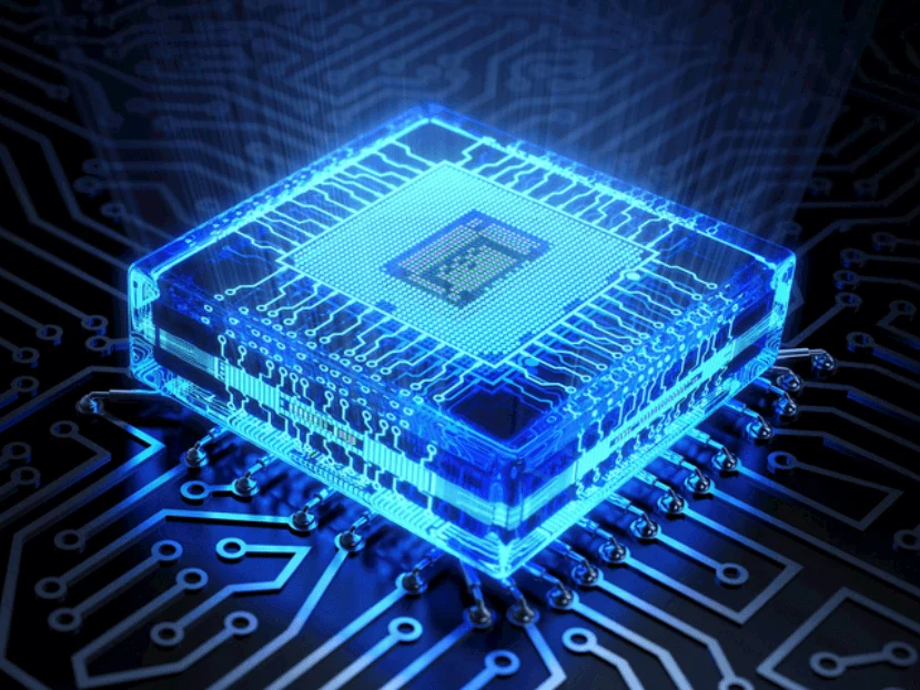
    – Huawei plans to reach TSMC’s 1.4 nm class through logic folding and advanced stacking, aiming for high transistor density without relying on EUV lithography.
    – China aims to field a functional EUV tool by 2031, plus techniques like SAQP, to move toward 5 nm and denser silicon with SMIC and Huawei.
    – Cooling and thermal management will be a critical challenge for stacked designs, requiring effective solutions within a five-year window.


    In this year, SMIC, china’s leading semiconductor manufacturing foundry, sits behind TSMC, Samsung Foundry and Intel by more than a few nodes, and that gap isn’t vanishing soon, though it might shrink. Huawei has announced it plans to compete with TSMC’s 1.4 nm node in 2031, which would still trail by a generation or so, but could keep China’s tech ecosystem reasonably aligned with Western peers.

    Logic Folding and the Path to Higher Density

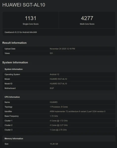
    paragraph with a slightly different voice explains how logic folding would work. Huawei says it will use this approach to stack two chips on top of each other, meaning more transistor density within the same die area without relying on smaller patterning techniques. This avoids immediate reliance on EUV tools, which China currently lacks, at least in present capabilities. The next-gen Kirin 2026 is pitched as among the first commercial chips to employ logic folding.

    EUV Progress and 2 nm Ambitions

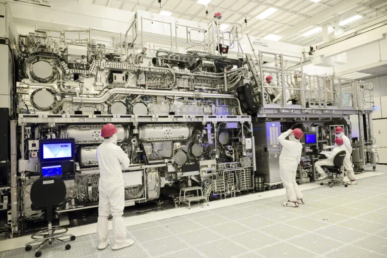
    Huawei notes that China has allegedly assembled a partially functional EUV machine with input from ex-ASML engineers. It isn’t fully operational yet, but could be by 2031. Paired with Huawei’s ongoing push to conquer the 2 nm barrier using methods like SAQP, this combination might enable Huawei and SMIC to challenge the 5 nm barrier and achieve denser silicon.

    • Cooling remains a critical challenge with stacked designs that generate more heat than traditional layouts.
    • The timeline remains uncertain, but Huawei has five years to resolve process inefficiencies.
    • Progress to date suggests uneven but notable advances in process technology.

    Huawei acknowledges the cooling challenge but stresses that for now it is still early to judge the overall feasibility, and that the strategic plan spans several years to iron out the technological kinks and optimize yields. The company asserts that the momentum is sufficient to keep expectations realistic while pursuing ambitious goals.

    Sources
  • China Develops Successful Prototype of EUV Machine

    China Develops Successful Prototype of EUV Machine

    Key Takeaways

    1. China has developed an EUV lithography machine in Shenzhen with help from ex-ASML engineers, marking a significant advancement in its chipmaking capabilities.

    2. The EUV machine is not yet ready for chip production, with full functionality expected by 2028 or 2030, while competitors may advance to high-NA EUV technology.

    3. China will need to produce the EUV machine’s components domestically and acquire used parts from other vendors due to the lack of official support from ASML.

    4. China has previously relied on older DUV machines to create advanced chips, pushing their limits to produce 5-nm-class chips.

    5. Despite this achievement, China faces major challenges in scaling production and navigating the complexities of new technology.


    A recent report from Reuters reveals that China has achieved a major milestone by developing an EUV (Extreme Ultraviolet) lithography machine at a lab in Shenzhen, with help from several ex-ASML engineers. This advancement validates earlier speculations and represents a crucial step forward in China’s chipmaking capabilities. It could enable Chinese firms like SMIC to create advanced chips that could rival those produced by TSMC, Intel, and Samsung. The project was reportedly kept under wraps, with the engineers working using pseudonyms.

    Future Challenges Ahead

    Despite this progress, the EUV machine still doesn’t have the ability to manufacture chips just yet. It is anticipated to reach full functionality by 2028 or potentially as late as 2030. By that time, industry rivals are expected to have moved on to high-NA EUV, the next-gen lithography technology created by ASML. Furthermore, scaling up production will be a tough task, as China will need to produce everything domestically due to ASML’s absence of official backing. To make matters more complicated, it must also acquire used components from different vendors, including Nikon and Canon.

    Relying on Older Technology

    Up until this point, China has depended on older DUV (Deep Ultraviolet) machines, which are the only models it can legally obtain from ASML. SMIC’s N+3 node has pushed DUV beyond its traditional limits by creating 5-nm-class chips like the Kirin 9030. There was even a recent patent that explored pushing the technology down to 2 nm. However, with the new EUV development, this may not be necessary due to the technology’s complexity and low yield rates.

    In conclusion, this report signifies a notable achievement for China, but significant hurdles remain in the way of fully realizing its chipmaking ambitions.

    Source:
    Link


  • Kirin 9030: SMIC’s First 5nm Smartphone SoC Appears on Geekbench

    Kirin 9030: SMIC’s First 5nm Smartphone SoC Appears on Geekbench

    Key Takeaways

    1. SMIC has successfully developed its first 5 nm-grade smartphone SoC, the Kirin 9030, using the N+3 process node.
    2. The Kirin 9030 features a high transistor density of about 125 Mtr/mm², comparable to Samsung’s 5LPE node.
    3. The chip is tested with the Huawei Mate 80 Pro Max, featuring a CPU with varying core speeds and a Maleoon 935 GPU.
    4. Geekbench scores for the Kirin 9030 are 1,131 (single-core) and 4,277 (multi-core), though these do not reflect its full potential.
    5. Despite advancements, the Kirin 9030 is expected to lag behind competitors like Snapdragon 8 Elite Gen 5 and MediaTek Dimensity.


    SMIC has made a notable advancement in its ability to produce semiconductors. The company has successfully created its first 5 nm-grade smartphone System on Chip (SoC) using its N+3 process node, which has been in the works since last year. With an impressive transistor density of about 125 Mtr/mm², this chip can stand alongside Samsung’s 5LPE node. This particular chip is the Kirin 9030, which will be the driving force behind the new Huawei Mate 80 series smartphones.

    Specifications Revealed

    Recently, the Kirin 9030 was found on Geekbench while being tested with the Huawei Mate 80 Pro Max (model HUAWEI SGT-AL10), which comes equipped with 16 GB of RAM. The chip includes one primary CPU core (likely from the Taishan family) running at 2.75 GHz, along with four additional cores clocked at 2.27 GHz and another four cores at 1.72 GHz. Additionally, it boasts a Maleoon 935 GPU, although detailed specifications for this GPU remain unclear.

    Performance Insights

    In the Geekbench tests, the Kirin 9030 achieved scores of 1,131 for single-core and 4,277 for multi-core performance. A leaker known as Digital Chat Station on Weibo pointed out that these results do not fully represent the chip’s capabilities, as it was not operating at its maximum speed during testing. Even when at full capacity, the Kirin 9030 is expected to fall short compared to competitors like the Snapdragon 8 Elite Gen 5 and MediaTek Dimensity, which is understandable due to its significant process node disadvantage.

    Conclusion

    In summary, while SMIC’s Kirin 9030 marks a step forward in semiconductor technology, it still has a way to go before matching leading contenders in the market. The developments in the Huawei Mate 80 series will be interesting to follow, particularly as they showcase this new chip’s potential.

    Source:
    Link


  • Lenovo Warns of PC Price Hikes in 2026 Amid AI Memory Shortages

    Lenovo Warns of PC Price Hikes in 2026 Amid AI Memory Shortages

    Key Takeaways

    1. Lenovo has increased its inventory levels by 50% to manage shortages in various memory products.
    2. The company aims to maintain strong sales by keeping product prices stable until the end of 2025.
    3. The AI sector’s demand is worsening memory shortages, which may lead to higher production costs and consumer prices.
    4. Future supply chain challenges are expected, with potential impacts on electronics and automotive chip availability in 2026.
    5. Lenovo has sufficient inventory and long-term contracts for 2026 but must balance pricing and availability moving forward.


    The Beijing-based computer manufacturer has boosted its inventory levels by 50 percent, as per CFO Winston Cheng’s comments to Bloomberg TV. This increase in stock has enabled Lenovo to navigate the significant shortages in DRAM, LPDDR, DDR, GDDR, and HBM that have affected the industry during the last quarter of 2025.

    Maintaining Sales Momentum

    Cheng mentioned that Lenovo aims to sustain its strong sales performance through the end of 2025 by keeping product prices stable. This strategy is crucial for ensuring continued consumer interest.

    Impact of AI on Supply Chain

    The demand from the AI sector is amplifying the shortage of memory products due to its high demand for storage components. This situation is likely to exert pressure on supply chains and raise production costs, which may lead to higher prices for consumer electronics. Suppliers and industry experts caution that items like laptops, PCs, and smartphones could see increased costs.

    Future Challenges for the Electronics Market

    According to Bloomberg, the Chinese chip manufacturer SMIC anticipates that the availability of electronics and automotive chips will be affected by memory shortages in 2026. Additionally, the well-known phone manufacturer Xiaomi has also alerted consumers about potential price hikes for its devices next year due to similar supply chain issues.

    Lenovo has previously disclosed that it has sufficient inventory for 2026 and has secured long-term contracts. However, Cheng pointed out that even with these advantages, Lenovo will need to find a balance between pricing and availability in the upcoming year.

    Source:
    Link


  • China’s Foundry Capacity Expected to Reach 30% by 2030

    China’s Foundry Capacity Expected to Reach 30% by 2030

    Key Takeaways

    1. By 2030, Mainland China’s semiconductor foundry capacity is projected to reach 30%, surpassing Taiwan’s stable 23%.
    2. China’s growth is driven by state-supported funding, particularly from the “Big Fund,” which supports domestic companies like SMIC and Hua Hong Semiconductor.
    3. Three new fab projects in China are set to begin in 2025, focusing on crucial mature nodes (8 nm to 45 nm) for various industries.
    4. China faces challenges in producing leading-edge products, with SMIC struggling to achieve consistent 5 nm processes while competitors advance to 2 nm.
    5. The shift in global semiconductor capacity reduces reliance on Taiwan and shows that market share does not guarantee technological leadership.


    According to new estimates from Yole Group, it appears that Mainland China is on track to surpass Taiwan in the global semiconductor foundry capacity by the time this decade concludes. The research company anticipates that by 2030, China will hold 30 percent of the worldwide capacity, an increase from 21 percent this year. Meanwhile, Taiwan’s share is expected to remain stable at about 23 percent. South Korea, Japan, and the United States follow behind with shares of 19 percent, 13 percent, and 10 percent, respectively.

    The Driving Force Behind Change

    The reason behind this transformation is largely due to Beijing’s “whole-nation” approach. The state-supported funding from the China Integrated Circuit Industry Investment Fund—commonly referred to as the “Big Fund”—has played a significant role in establishing national players like Semiconductor Manufacturing International Corp (SMIC) and Hua Hong Semiconductor. Currently, domestic companies are responsible for around 15 percent of China’s foundry output, and Yole forecasts that this percentage will increase significantly as new fabs become operational.

    Construction Trends Align with Projections

    Data regarding construction backs up these predictions. SEMI, a U.S. industry group, has reported that three new fab projects in China are expected to commence in 2025, which accounts for one-sixth of the total worldwide. Many of these projects are aimed at mature nodes ranging from 8 nm to 45 nm, a capacity that remains crucial for automotive, industrial control systems, and the growing Internet-of-Things market.

    Challenges Ahead for China

    However, China faces challenges when it comes to leading-edge products. SMIC has not yet proven a consistent 5 nm process, two years after it launched its first 7 nm chips in Huawei devices. On the other hand, Taiwan Semiconductor Manufacturing Co. and Samsung Electronics are pushing rapidly towards mass production at 2 nm. Lacking similar lithography tools—due to U.S. export restrictions—Chinese fabs are likely to concentrate on volume production instead of cutting-edge density.

    In conclusion, the shift in capacity is significant. It diminishes the global reliance on a few Taiwanese locations and indicates that merely having market share does not assure technological dominance anymore.

    Source:
    Link

  • Huawei Developing Two New 3nm Chips for Future Devices

    Huawei Developing Two New 3nm Chips for Future Devices

    Key Takeaways

    1. SMIC has successfully produced its first 5 nm chip, the Kirin X90 for Huawei, using DUV machines due to trade restrictions on EUV technology.
    2. Huawei is researching a 3 nm chip using GAA FET technology, aiming for tape-out by 2026 and mass production by 2027.
    3. Yield rates for the 5 nm chip are low at 20%, and the 3 nm chips are expected to have even lower rates due to complex DUV multi-patterning.
    4. China is investing in developing its own EUV machines, with reports suggesting Huawei is testing EUV technology for potential mass production by 2026.
    5. Advancements in EUV technology are likely to be kept secret, with significant funding of $37 billion allocated for its development.


    If the whispers from China are true, SMIC has made a significant breakthrough by producing its first 5 nm chip for Huawei, named the Kirin X90. This accomplishment was achieved without the advanced EUV machines from ASML. Instead, they relied on less powerful DUV machines due to trade limitations. A recent article from UDN sheds light on Huawei’s upcoming strategies regarding its semiconductor sector.

    Future Semiconductor Developments

    Huawei is now delving into research for a 3 nm node based on GAA FET technology, which they expect to have ready for tape-out around 2026. If everything goes as planned, they aim to kick off mass production by 2027. In addition, there are also investigations into carbon nanotube-based 3 nm chips, though there’s no update on their development status.

    Challenges Ahead

    Yet, yield rates will remain a concern. The aforementioned 5 nm node reportedly has a low yield rate of just 20%, and this number is expected to decline even further for the 3 nm chips due to the increased complexity of DUV multi-patterning. However, this situation could improve if China manages to transition to EUV technology like TSMC, Samsung, and Intel Foundry.

    China is already putting effort into creating its own EUV machines. An X user, @zephyr_z9, who has insights into the Chinese semiconductor industry, notes that Huawei is testing EUV technology, which is anticipated to be ready for mass production by 2026. On the other hand, former ASML engineer @lithos_graphein argues that this is improbable, stating, “ASML’s moat is massive and uncontested.”

    Secrecy in Progress

    Still, even if China had EUV tools available, they likely wouldn’t make this information public. Reports indicate that $37 billion has been designated for the development of EUV technology, and any advancements will likely be kept secret, similar to what occurred with the Kirin 9010 and its later versions.

    Source:
    Link

  • SMIC Yield Issues Rise Due to U.S. Sanctions on Tool Servicing

    SMIC Yield Issues Rise Due to U.S. Sanctions on Tool Servicing

    Key Takeaways

    1. SMIC expects a revenue dip of up to 6% in Q2 due to equipment maintenance disruptions.
    2. U.S. export restrictions have forced unqualified SMIC engineers to manage advanced tool maintenance, increasing risk of further disruptions.
    3. In Q1 2025, SMIC reported $2.247 billion in revenue, a 1.8% increase, primarily driven by wafer sales.
    4. Equipment issues have diverted $30 million to $75 million from R&D, but SMIC maintains a $7.5 billion capital expenditure plan.
    5. Co-CEO Haijun Zhao noted that tariff impacts on revenue are minimal, but increasing prices may affect demand later in the year.


    Semiconductor Manufacturing International Corporation (SMIC) is expecting a revenue dip of up to six percent for the second quarter due to disruptions from equipment maintenance and validation. A mishap during their annual maintenance, along with problems found in newly set up tools, has led to a decrease in sellable output, without affecting the average selling prices.

    Maintenance Challenges

    U.S. export restrictions preventing American suppliers from servicing advanced wafer fabrication tools in China have compelled SMIC engineers, who don’t have formal qualifications for some tasks, to handle maintenance themselves. This situation raises the risk of further disruptions and could lead to lower yield quality.

    First Quarter Performance

    In the first quarter of 2025, SMIC reported revenue of $2.247 billion, reflecting a 1.8 percent increase from the previous quarter. Wafer sales made up 95.2 percent of this total, thanks to an 18 percent rise in shipments of 200-millimeter wafers and a two percent growth in 300-millimeter volumes. Factory utilization increased to 89.6 percent, helping to mitigate the effects of lower unit prices and rising depreciation costs on profit margins.

    Financial Implications

    Addressing the issues with the faulty equipment has already redirected between $30 million and $75 million from research and development. Nevertheless, management is sticking to a bold $7.5 billion capital-expenditure plan for the year. Executives believe the current impact of tariffs is “minor,” although they admit that increased prices downstream might limit demand in the latter half of the year.

    Co-CEO Haijun Zhao mentioned that close collaboration with partners and received tariff exemptions have helped to keep the direct revenue impact from trade policies below one percent. The company is still closely watching customer demand due to the ongoing geopolitical uncertainties.

    Source:
    Link

  • China Achieves 5nm Chip Tech Without EUV: SMIC Defies Sanctions

    China Achieves 5nm Chip Tech Without EUV: SMIC Defies Sanctions

    Key Takeaways

    1. SMIC has successfully produced 5nm chips using older DUV equipment instead of EUV lithography.
    2. The technique employed is called Self-Aligned Quadruple Patterning (SAQP), which simulates EUV accuracy.
    3. This achievement challenges the belief that EUV is essential for producing advanced chips below 7nm.
    4. The production process is more time-consuming, error-prone, and costly but has resulted in functional 5nm-class chips.
    5. The new chips are already integrated into devices like the Huawei Mate 60, outperforming competitors with features like satellite call capabilities.


    In a significant development that could transform the worldwide semiconductor market, China’s Semiconductor Manufacturing International Corporation (SMIC) has seemingly succeeded in producing 5nm chips without relying on extreme ultraviolet (EUV) lithography.

    Innovative Techniques Used

    Instead, SMIC has employed older deep ultraviolet (DUV) equipment, combined with a complex technique called Self-Aligned Quadruple Patterning (SAQP). This achievement, highlighted in several tweets by semiconductor expert William Huo on X, represents not just a technological advance but also a bold message in the realm of geopolitics.

    Overcoming Challenges

    Traditionally, the industry has believed that EUV lithography, which is only available from the Dutch firm ASML, was essential for producing chips at 5nm and lower. With the limitations on EUV access imposed by the U.S. and its partners, many experts thought that China would be unable to progress beyond the 7nm level. However, SMIC has managed to forge ahead, using intensive DUV methods to extract every possible nanometer from their older equipment.

    Results of the Breakthrough

    According to Huo, this process involved layering several lithography and etching steps, particularly utilizing SAQP to simulate the accuracy of EUV. Although this technique is more time-consuming, prone to mistakes, and costly, it proves effective. The outcome? A functioning 5nm-class chip, which is reportedly already integrated into devices such as the Kirin 9000S-powered Huawei Mate 60, that notably outperformed the iPhone 15 by providing satellite call capabilities first.

  • Huawei Ascend 920: Nvidia H20 Replacement Expected This Year

    Huawei Ascend 920: Nvidia H20 Replacement Expected This Year

    Key Takeaways

    1. Huawei is finding new ways to obtain advanced hardware for AI training despite TSMC blocking its chip production efforts.
    2. The newly released Ascend 910C shows potential to compete with Nvidia, but has significant limitations.
    3. The Ascend 920 chip is expected to launch soon, built using SMIC’s 6 nm class N+3 technology, with mass production starting in the latter half of 2025.
    4. The Ascend 920 is designed to deliver 900 TFLOPS of BF16 performance and 4,000 GB/s memory bandwidth with HBM3 memory.
    5. SMIC’s 6 nm class node may also be used in future products like Kirin chips for Huawei smartphones, with whispers of a developing 5 nm class node.


    Even with TSMC blocking Huawei’s efforts to produce its Ascend 910B chips using advanced technology, the large Chinese company has discovered new methods to obtain top-tier hardware for AI training. The Ascend 910C was released shortly after that setback, and a detailed analysis from SemiAnalysis indicates that it has the potential to compete with Nvidia, though there are several important limitations. Recently, a report from DigiTimes indicates that its successor, the Ascend 920, is expected to launch soon.

    Manufacturing Insights

    Well-known leaker Jukanlosreve on X has shared that the Ascend 920 will be built using SMIC’s 6 nm class N+3 technology. Mass production is set to begin in the latter half of 2025. The chip is said to deliver 900 TFLOPS of (presumably) BF16 performance and boasts a memory bandwidth of 4,000 GB/s, made possible by HBM3 memory. It is designed to replace Nvidia’s Hopper-based H20 chip, which has recently been banned for use in China.

    Future Developments

    The introduction of the Ascend 920 also marks the debut of SMIC’s new 6 nm class node, which is likely to be implemented in other products, including Kirin chips for Huawei smartphones. Although the previously anticipated Kirin 9100 didn’t succeed, there are indications that it may still launch later this year. Additionally, there have been whispers about a 5 nm class SMIC node under development, but advancements in that area may be sluggish due to limited access to EUV machinery.

    Source:
    Link

  • Huawei Outsmarts US Chip Ban: Report on Breakthrough Chip Utilizing US Tech

    Huawei Outsmarts US Chip Ban: Report on Breakthrough Chip Utilizing US Tech

    Despite facing restrictions from the United States on providing advanced chip technology to China, Huawei successfully developed a more potent chip for its Mate 60 Pro smartphone by leveraging technology from American companies.

    Utilization of US Technology by Huawei and SMIC

    An earlier report highlighted SMIC's utilization of ASML's technology in the past. Recent reports from Bloomberg reveal that Huawei, in collaboration with its chip manufacturing partner SMIC, incorporated technology from Applied Materials and Lam Research, both based in California, to craft a 7-nanometer chip. While not the most cutting-edge chip in existence, it outperforms what the US had intended for its rival in the ongoing chip conflict. This development follows a previous Bloomberg report from October 2023, which mentioned SMIC using ASML's technology for a different advanced Huawei chip.

    Acquisition of US Technology by SMIC

    SMIC purportedly acquired the US technology before the US Department of Commerce enforced a ban in October 2022. This ban aimed to prevent US companies from supplying advanced chipmaking equipment and chips to Chinese entities. Subsequent restrictions in November 2022 further hindered equipment sales approvals to Huawei and other Chinese firms, citing national security reasons.

    Impact on Market Demand

    Although there is no conclusive evidence from the US Commerce Department regarding SMIC's mass production of these advanced chips, Huawei witnessed robust initial demand for its Mate 60 series in the first six weeks of 2024. Concurrently, Apple experienced a notable 24% decline in iPhone sales in China during the same period, while overall smartphone sales in China decreased by 7%.