Tag: AMD Zen 6

  • Intel’s Nova Lake Brings IPC Gains, Could Beat Zen 6 in 2023

    Intel’s Nova Lake Brings IPC Gains, Could Beat Zen 6 in 2023

    Key Takeaway

    1. Next-gen Intel Core Ultra and AMD Zen 6 CPUs are delayed until 2027, but are expected to feature more cores, higher clock speeds, and IPC improvements.
    2. Intel Nova Lake CPUs may outperform AMD Zen 6 in IPC uplift, while AMD may have faster clock speeds.
    3. Intel’s upcoming chips could potentially surpass AMD in all categories, including gaming and multi-threaded workloads, with possible improvements in cache sizes and architectural design.

    Upcoming CPU Releases from Intel and AMD

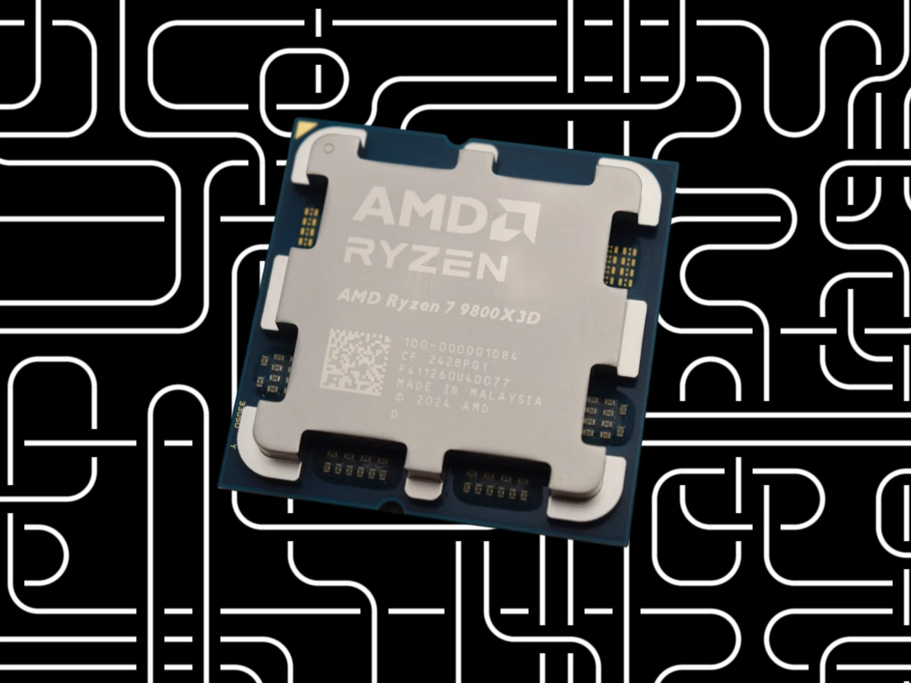
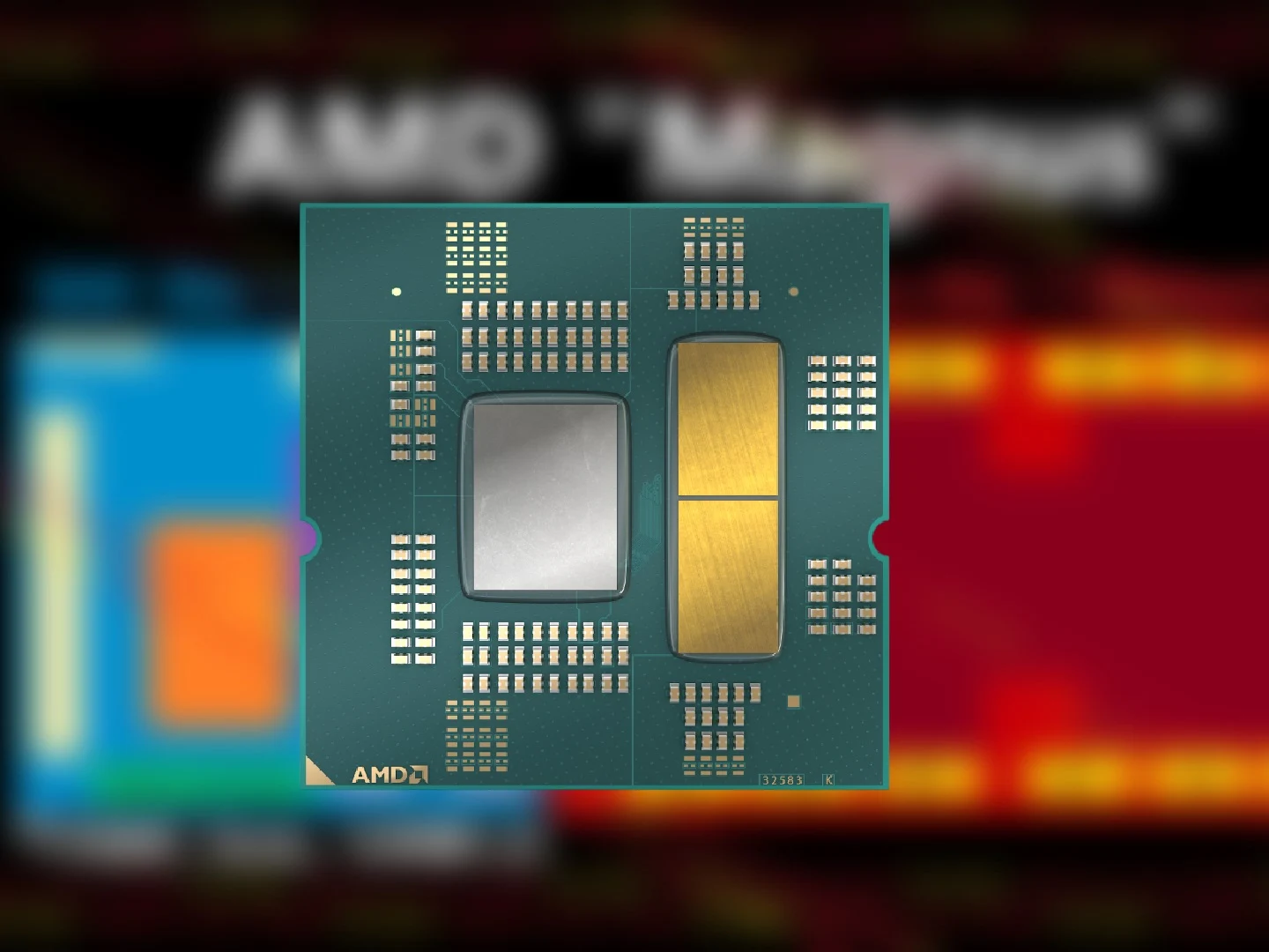
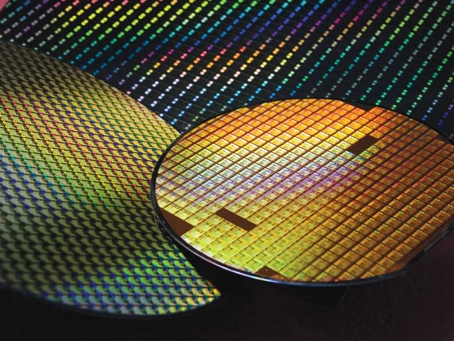
    The latest rumors and leaks about the upcoming Intel Nova Lake and AMD Zen 6 processors have significantly delayed the official launches to 2027. These new chips are expected to boast more cores, faster clock speeds, and considerable IPC improvements, which might result in massive boosts in performance compared to the current CPUs.

    Performance Expectations and Comparisons

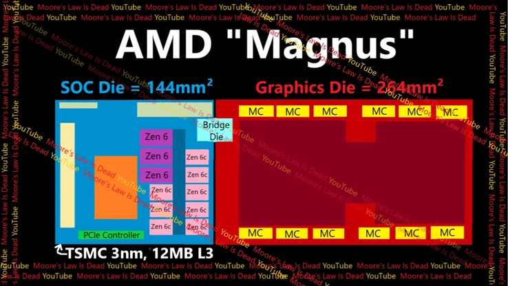
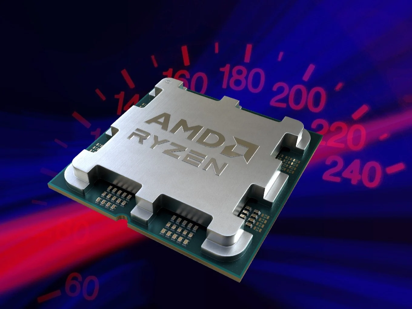
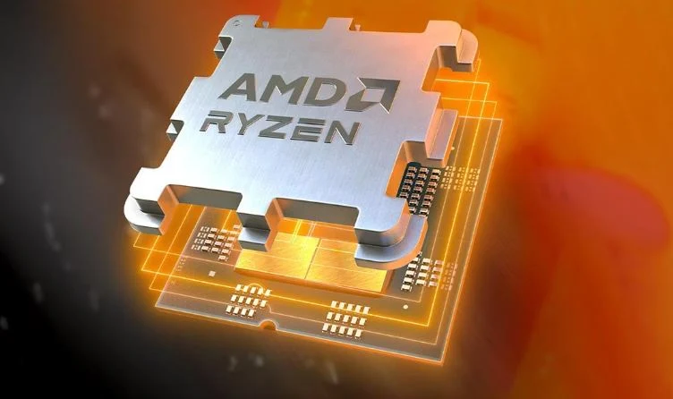
    According to leaker HXL (@9550Pro) on social media, the Intel Nova Lake CPUs could potentially surpass AMD Zen 6 in terms of IPC improvements from one generation to the next, specifically citing the IPC uplift of the Coyote Cove P-cores. Meanwhile, HXL suggests that AMD Zen 6 might sport higher clock speeds than Intel Nova Lake, creating an interesting flip in who holds the performance crown. It’s noteworthy that this is a change from the previous generation, where Intel’s 14th-gen processors were pushing such insane clock speeds as 6 GHz right out of the box.

    Specs and Potential Market Impact

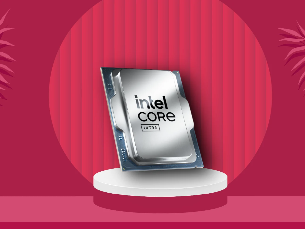
    With up to 52 cores and higher clocks, Intel’s Nova Lake Core Ultra 400 desktop CPUs might outshine AMD in all categories, especially with better IPC uplift. Rumors also hint at some chips having large Last Level Cache (bLLC), which could diminish AMD’s gaming edge with their X3D series. Additionally, Intel’s recent architectural improvements seen in Arrow Lake Refresh Core Ultra 200S Plus processors have led to notable performance increases over the original Core Ultra 200 Arrow Lake chips, hinting that such upgrades could be applied to Nova Lake as well.

    Future of high-end desktop computing

    In conclusion, it’s not unlikely that Intel’s Nova Lake lineup will dominate many areas, from gaming single-core workloads to heavily threaded applications. Some industry insiders, like SiliconFly, have even proclaimed that Zen 6 is already ready, but Nova Lake CPUs might quickly catch up to Apple’s M5 chips in single-core performance and outperform them in multi-core tasks.

  • AMD Zen 6 vs Intel Nova Lake: Gaming Battle with 288MB V-Cache

    AMD Zen 6 vs Intel Nova Lake: Gaming Battle with 288MB V-Cache

    Key Takeaways

    1. AMD Zen 6 CPUs may feature up to 144 MB of 3D V-Cache, a significant increase from the previously expected 96 MB.
    2. Intel’s Nova Lake CPUs could offer up to 288 MB of last-level cache, potentially giving Intel an advantage in gaming performance.
    3. Both AMD and Intel’s high cache options are expected to come with high price tags, especially for models with 288 MB of cache.
    4. The performance comparison between AMD Zen 6 and Intel Nova Lake will depend on factors like per-core IPC improvements and clock speeds.
    5. Current performance metrics for both CPU lines have not been disclosed, leaving the competition outcome uncertain.


    The AMD Zen 6 CPUs were earlier thought to have 96 MB of 3D V-Cache, which is a 50% rise from the 64 MB found in the Ryzen 7 9800X3D. With a possible 10%+ boost in single-core IPC, it seemed like AMD Zen 6 would hold onto its gaming title. Nonetheless, Intel Nova Lake might bring up to 288 MB of last-level “bLLC” cache, possibly giving Intel the upper hand in gaming.

    AMD’s Surprise Move

    Recent leaks suggest AMD may have something special up its sleeve. According to leaker HXL, the Zen 6 CPUs may feature a single 3D V-Cache die with 144 MB, rather than the previously speculated 96 MB. This means that Zen 6 X3D models could potentially offer 144 MB of last-level cache, while versions with dual 3D V-Cache dies might provide a whopping 288 MB of additional L3 cache.

    Cache Comparison with Intel

    The 3D V-Cache setup for Zen 6 CPUs aligns with the Intel Nova Lake CPUs. Reports indicate that NVL-S desktop chips featuring dual-bLLC could also offer 288 MB of last-level cache. However, such a substantial increase in L3 cache might come with a hefty price tag. So, prepare to shell out some serious money if you’re interested in Zen 6 or Nova Lake CPUs with 288 MB of last-level cache.

    Even with pricing concerns, having 288 MB of extra L3 cache is significant for gaming. The Ryzen 7 9800X3D already demonstrates the impact of a 64 MB section of 3D V-Cache on gaming performance. Therefore, we can anticipate that both Intel Nova Lake and AMD Zen 6 CPUs with this extra L3 cache will provide outstanding gaming experiences.

    The Final Showdown

    At this point, it’s hard to determine which company will take the lead since Intel and AMD haven’t disclosed any performance metrics yet. If both Intel Nova Lake and AMD Zen 6 have the same amount of last-level cache, the outcome of the gaming performance clash will hinge on factors like per-core IPC improvements and clock speeds.

    Source:
    Link


  • Xbox Magnus Leak: Next-Gen 4K120 Gaming with AMD Zen 6

    Xbox Magnus Leak: Next-Gen 4K120 Gaming with AMD Zen 6

    Key Takeaways

    1. Microsoft’s upcoming Xbox, codenamed Magnus, will feature AMD’s Zen 6 CPU cores and RDNA 5 graphics technology, promising performance up to twice that of the PlayStation 5 Pro.
    2. The Magnus APU will use a two-chiplet architecture with an AT2 GPU die, including 68 active compute units and a 192-bit GDDR7 memory interface.
    3. Expected performance is comparable to a Radeon-class GPU similar to an RTX 5080, with 50 to 100 percent higher performance than the PS5 Pro for various tasks.
    4. The console is anticipated to support features like FSR upscaling, ray tracing, and backwards compatibility with older Xbox games, with a potential launch price between $500 and $600.
    5. The Magnus design could significantly impact the mid-range PC market by using the same technology found in desktop GPUs, with more details on pricing and release dates expected soon.


    A recent leak from Moore’s Law is Dead indicates that Microsoft’s upcoming Xbox, known internally as Magnus, is set to incorporate AMD’s Zen 6 CPU cores alongside RDNA 5 graphics technology. This combination is projected to provide performance that could be up to twice as powerful as the PlayStation 5 Pro. The release of this system could happen as soon as late 2026 or in 2027.

    Technical Details

    The leaked information points out that the Magnus APU will feature a two-chiplet architecture that revolves around the AT2 GPU die, which will also be utilized in AMD’s mid-tier desktop graphics cards. This graphics unit is believed to include 68 active compute units and will have a 192-bit GDDR7 memory interface. Meanwhile, the CPU will be based on a cutting-edge 3nm Zen 6 design. Moore’s Law is Dead estimates that the performance will be comparable to a Radeon-class GPU akin to an RTX 5080, potentially offering between 50 to 100 percent higher performance than the PS5 Pro, depending on the specific tasks.

    Cost and Features

    Utilizing the AT2 die for both the console and desktop graphics could help Microsoft reduce manufacturing costs over time, as well as enhance driver support. The Magnus is also anticipated to include features like FSR upscaling, ray tracing capabilities, and backwards compatibility with older Xbox games. While the exact pricing remains unclear, there is speculation suggesting a launch price might fall within the $500 to $600 range, with a minimum of 32GB RAM to facilitate high-resolution gaming at 120Hz.

    Future Outlook

    If these leaks are accurate, the Magnus design could mark a major advancement for Xbox, utilizing AMD’s next-gen technologies to focus on high-refresh 4K gaming. This could also shake up the mid-range PC market by using the same silicon found in desktop GPUs. More detailed information, such as pricing and release dates, is likely to surface in the upcoming months as development progresses.

    Source:
    Link

  • AMD Zen 6 Magnus APU Leaks: PS6 and Next-Gen Xbox Features

    AMD Zen 6 Magnus APU Leaks: PS6 and Next-Gen Xbox Features

    Key Takeaways

    1. The upcoming AMD Zen 6 CPUs, including the “Magnus” APU, feature innovative designs like 12-core CCDs and dual-layer 3D V-Cache.
    2. The “Magnus” Zen 6 APU consists of 3 Zen 6 cores and 8 Zen 6c cores, totaling 11 cores, and is built on TSMC’s 3 nm technology with 12 MB of L3 cache.
    3. The APU’s large Graphics Die measures 264 mm² and includes a 384-bit wide bus for enhanced memory bandwidth, targeting high-performance gaming.
    4. Speculation exists on whether the Magnus APU will be used in the next PlayStation or Xbox, with differing opinions on its cost-effectiveness for each console.
    5. The hardware associated with the Zen 6 Magnus APU is expected to be expensive, indicating that future consoles like the PS6 or next Xbox may have a high price point.


    There has been an overflow of leaks and speculation surrounding the design and specifications of AMD’s upcoming Zen 6 CPUs. A lot of this intel, such as details about 12-core CCDs, dual-layer 3D V-Cache, and remarkable clock speeds, is thanks to Moore’s Law Is Dead. Recently, the leaker shared a fresh video that reveals even more insights about Zen 6, including a thrilling new Zen 6 APU known as “Magnus.”

    Focus on the Magnus APU

    The entire video is certainly worth a watch (linked below), but we’re zeroing in on the “Magnus” Zen 6 APU. There’s a good chance this uniquely designed APU may find its way into next-generation gaming consoles.

    From a diagram presented by MLID in the video, the Zen 6 APU, codenamed “Magnus”, is said to have 3 Zen 6 cores and 8 Zen 6c cores, totaling an unusual 11 CPU cores. The System on Chip (SoC) that holds these cores is reported to be a sizable 144 mm², produced using the TSMC 3 nm technology, and includes 12 MB of L3 cache.

    Technical Specifications

    Allegedly, the SoC die connects to the Graphics Die via a “Bridge Die.” The Graphics Die appears to be a massive 264 mm². The integrated GPU (iGPU) in this Zen 6 APU boasts a 384-bit wide bus. This aspect is crucial, as memory bandwidth often poses a significant limitation for iGPUs designed for gaming.

    With both the SoC and Graphics chiplets being quite large and a memory bus wider than Strix Halo’s 256-bit, it’s clear that the Magnus APU isn’t aimed at budget-friendly setups. MLID theorizes that, given the codename and other hints, the Zen 6 Magnus APU could potentially serve as the APU for the PS6. It’s already known that Sony is collaborating with AMD to develop the PS6’s custom APU, making a large iGPU a logical choice.

    Speculations about Console Compatibility

    Nonetheless, leaker Kepler_L2 disagrees on X, suggesting that “Magnus” doesn’t align with Sony’s typical codenames, hinting that this APU may be intended for the next Xbox instead. This leaker also points out that “the design overall looks too pricey to be the PS6 too. Cerny tends to be more cautious with die size.”

    If we consider that the next Xbox will operate on Windows and that Microsoft is working on multiple Xbox models, a high-end Xbox featuring the Zen 6 Magnus APU makes sense. Kepler_L2 predicts that with “>400mm² of N3P (or perhaps even N3P+N2P?) plus likely 36GB of GDDR7,” the upcoming Xbox could surpass $1,500.

    Regardless of which next-gen console incorporates the Zen 6 Magnus APU, one thing is clear: the hardware isn’t going to come cheap. So, if you’re already frustrated with the pricing of existing consoles like the PS5 Pro, brace yourself for the PS6 or the next Xbox, which may be even pricier.

    Source:
    Link


  • AMD Zen 6 IPC Leak: Exciting 3D V-Cache Boosts Performance

    AMD Zen 6 IPC Leak: Exciting 3D V-Cache Boosts Performance

    Key Takeaways

    1. Upcoming CPU Releases: AMD Zen 6 and Intel Nova Lake are set to be the leading desktop CPU designs, expected around 2026.

    2. Performance Improvements: Intel’s Nova Lake may achieve a 10% boost in single-core performance and up to 60% in multi-core performance compared to Arrow Lake-S CPUs, while Zen 6 is expected to have a 7 to 9% uplift in Floating Point IPC.

    3. Enhanced Cache Features: Zen 6 is rumored to support increased 3D V-Cache, potentially reaching 96 MB or more, with configurations that could allow up to 240 MB of L3 cache.

    4. Gaming Focus: Zen 6 is particularly aimed at gamers, with features like boost clocks exceeding 6 GHz and improved 3D V-Cache for better gaming performance.

    5. Current Options: AMD’s existing Zen 5 processors, like the Ryzen 5 9600X, are available at good prices for those who need upgrades before Zen 6 is released.


    AMD Zen 6 and Intel Nova Lake are likely going to be the leading new desktop CPU designs set to release around 2026. Intel’s Nova Lake is said to feature as much as 56 cores, new P/E cores, a low-power core island, and additional enhancements. On the other hand, AMD is gearing up for Zen 6, which promises significant upgrades, such as possibly astonishing boost clocks, increased core counts, and a state-of-the-art TSMC fabrication process.

    Performance Expectations

    Leaked information suggests that Intel’s Nova Lake might deliver a 10% boost in single-core performance and as much as 60% improvement in multi-core performance compared to Arrow Lake-S CPUs. Unfortunately, we don’t have similar details for Zen 6 yet, as leaks on its performance have been limited.

    Early IPC Insights

    Moore’s Law Is Dead has filled this void by disclosing initial IPC (Instructions Per Cycle) figures for Zen 6. According to a source within AMD, retail Zen 6 CPUs are expected to provide a 7 to 9% uplift in Floating Point (FP) IPC compared to Zen 5.

    However, the source warned MLID that this number is “NOT the final claimed IPC that will consider gaming and other PPC uplift”. Therefore, the leaker suggests that the ultimate IPC enhancement, which includes gains from gaming and other tasks, might reach or surpass 10%.

    Cache and Gaming Focus

    We have previously noted that Zen 6 could support more than just 12-core CCDs; it is also expected to feature increased 3D V-Cache. An AMD source for MLID has confirmed that Zen 6 will include 96 MB of 3D V-Cache. The source also indicated that Zen 6 CPUs could utilize multiple layers of 3D V-Cache, allowing for configurations like 240 MB of L3 cache if AMD opts for two layers of 3D V-Cache.

    Zen 6 is said to be particularly aimed at gaming. Features like boost clocks exceeding 6 GHz and enhanced 3D V-Cache align well with AMD’s supposed strategy. Consequently, those looking to upgrade next year can anticipate notable improvements in gaming performance from generation to generation.

    Current Options

    If the wait is too long, many of AMD’s current-generation Zen 5 processors are available at attractive prices. For example, the 6-core Ryzen 5 9600X, which has shown impressive performance in our evaluations, is currently a great deal on Amazon.

    In conclusion, please keep in consideration that the information shared by MLID remains unverified until AMD officially announces Zen 6. Since Zen 6 is at least a year away, it’s unlikely that AMD will provide any definitive information in the near future.

    Source:
    Link


  • AMD Zen 6 Leak: Targeting Up to 7 GHz Boost for Gaming Performance

    AMD Zen 6 Leak: Targeting Up to 7 GHz Boost for Gaming Performance

    Key Takeaways

    1. AMD’s upcoming Zen 6 CPUs may reach clock speeds of 7 GHz or more, marking a significant increase over previous Ryzen chipsets.
    2. The Zen 6 architecture will feature a “two to three node jump” from Zen 5, improving architectural efficiency and transistor density.
    3. Zen 6 is expected to have 12 unified cores, while Intel’s Nova Lake may include 16 unified P-cores, raising concerns about high core counts in gaming.
    4. High core counts can lead to trade-offs, such as race conditions and rendering issues, complicating game development despite improvements in parallel workload handling.
    5. Low-power Zen 6 cores under 1 watt could enhance efficiency for devices like the Steam Deck, though there are concerns about compatibility with older games at high clock speeds.


    A recent leak from Moore’s Law Is Dead reveals that AMD’s upcoming Zen 6 CPUs might showcase significantly higher clock speeds than any Ryzen chipsets seen before. Although the precise figures aren’t made public, the leak, discussed by Tom Guinet and guest Jesse Brandon, hints at speeds that could reach or even exceed 7 GHz in certain situations, described as “as crazy as you think it is.”

    Next-Level Technology

    According to Tom, the Zen 6 architecture will represent a “two to three node jump” from Zen 5, indicating not only a remarkable increase in clock speeds but also a notable improvement in architectural efficiency and transistor density. The Zen 6 X3D versions are expected to incorporate extensive 3D V-Cache alongside these high clock speeds, potentially changing the gaming performance landscape, as Tom suggests.

    Core Count Competition

    During their discussion, Jesse pointed out that AMD is aiming for 12 unified cores in Zen 6, while Intel’s upcoming Nova Lake is anticipated to feature 16 unified P-cores.

    Additionally, they brought up worries from various game developers, especially those using Unreal Engine, about the long-term feasibility of very high core counts in consumer CPUs.

    Trade-offs in Performance

    While Unreal Engine 5.6 has improved in handling parallel workloads, Jesse claims this development often brings trade-offs. These trade-offs include more race conditions, rendering issues, and greater complexity, which complicates both development and debugging processes.

    Race conditions happen when multiple threads try to access or change the same data at once, causing unpredictable bugs that are hard to reproduce and resolve. Jesse believes that maintaining strong single-threaded performance and high clock speeds is vital for consistent gaming performance today.

    Low-Power Potential

    Tom also mentioned the exciting possibility of low-power Zen 6 cores that use less than 1 watt. He argues that such efficiency could make these cores suitable for devices like the Steam Deck or future gaming consoles. For context, the PS4 had a dedicated ARM chip for managing sleep mode and background tasks, and while the PS5 is suspected to follow a similar approach, there’s yet to be any official confirmation or teardown proof to confirm the existence of a dedicated ARM processor.

    Concerns were raised about possible compatibility issues with older games when operating at extremely high clock speeds, leading to a wider discussion about the balance between frequency and core counts. For a more detailed look and technical insights, be sure to check out the full video linked below.

    Source:
    Link

  • AMD Zen 6 CPUs Boost Clock Leaks Over 6.2 GHz

    AMD Zen 6 CPUs Boost Clock Leaks Over 6.2 GHz

    Key Takeaways

    1. AMD Zen 6 desktop CPUs are expected to launch next year with a 50% increase in cores compared to Zen 4 models.
    2. Boost clock speeds for Zen 6 CPUs may exceed 6 GHz, with speculation of reaching 6.5 GHz or higher.
    3. The same team that developed Zen 4, which achieved a boost frequency of 5.7 GHz, is working on Zen 6.
    4. AMD is utilizing the advanced TSMC N2 node, particularly N2X, for the Zen 6 processors.
    5. Claims about clock speeds should be viewed with skepticism until official confirmation is provided.


    The AMD Zen 6 desktop CPUs are anticipated to launch next year, featuring a 50% increase in cores compared to the Zen 4 models. This significant rise in core count is said to come along with a remarkable boost in core clock speeds as well.

    Exciting Boost Clocks Ahead

    Earlier in March, we shared that the AMD Zen 6 CPUs may achieve boost clocks as high as 6 GHz. Recently, Moore’s Law Is Dead has shared more insights about this potential upgrade in a new video (linked below).

    According to MLID, after chatting with various AMD sources, the company is aiming for a boost clock that exceeds 6 GHz for the Zen 6 processors. While MLID does not provide a specific boost frequency, they mention that it’s “so insane” the information might be hard for viewers to accept.

    Speculations on Clock Speed

    Nevertheless, MLID hints that the figure is not merely 6.1 or 6.2 GHz, but significantly higher. To give more background on the considerable speed jump from Zen 5 to Zen 6, the leaker claims that the same team responsible for Zen 4, which achieved a boost frequency of 5.7 GHz, is developing Zen 6. With AMD utilizing the cutting-edge TSMC N2 node, especially N2X, it’s conceivable that they could push Zen 6 CPUs to clock speeds of 6.5 GHz or even higher.

    It’s important to note, however, that these figures are targets and may not always be realized. The boost clocks for the Zen 6 desktop CPUs could turn out to be lower than what MLID suggests. Therefore, until there is official confirmation or solid proof, it’s wise to take MLID’s claims with some skepticism.

    Source:
    Link

  • TSMC 2nm Wafers Expected to See 10% Price Increase

    TSMC 2nm Wafers Expected to See 10% Price Increase

    Key Takeaways

    1. TSMC’s N2 node is in high demand from major companies like AMD, Nvidia, Apple, and Qualcomm, leading to higher pricing for wafers.
    2. Wafer prices are expected to rise further due to construction costs of fabs, economic uncertainty, and TSMC’s need to recover significant investments.
    3. The cost of TSMC’s 2 nm wafers is projected to increase by 10%, potentially reaching around $33,000 for a 300 mm wafer.
    4. Smaller OEMs might shift to older nodes (N3, N4) or consider Samsung Foundry’s 2 nm options due to rising TSMC prices.
    5. Intel’s innovative 18A and 14A nodes are becoming competitive alternatives, featuring technologies not available from TSMC and Samsung Foundry for several years.


    With the increasing demand from companies like AMD, Nvidia, Apple, Qualcomm, and even Intel, which has its own fabrication plants, TSMC’s N2 node is becoming one of the most wanted in recent times. This high demand allows the Taiwanese semiconductor manufacturer to set higher prices.

    Rising Wafer Prices

    A new report from Ctee suggests that wafer prices might rise even further in the upcoming weeks. Insiders believe this is due to the increasing expenses of constructing fabs in countries like the United States, the overall uncertainty in the global economy, and the need to recover some of the $38-42 billion that TSMC intends to invest this year for capital projects.

    Cost of TSMC’s 2 nm Wafers

    A wafer at TSMC’s 2 nm node is expected to be 10% pricier than previously. Last year, the estimated cost was around $30,000 for a 300 mm wafer, which means the new price could reach about $33,000. The report mentions that Nvidia’s CEO, Jensen Huang, finds TSMC’s advanced nodes to be “very worth it.”

    Nvidia plans to use the N2 node for its upcoming Rubin Next architecture. It will also be utilized in AMD’s Zen 6 processors, Apple’s A21 and M5 chips, MediaTek’s Dimensity SoC, and potentially even in the CPU tile of Intel’s Nova Lake desktop series.

    Smaller OEMs and Alternatives

    This situation might lead many smaller OEMs to consider older options like the N3 and N4 nodes. Alternatively, they may explore Samsung Foundry’s 2 nm offerings (SF2/SF2P), which Qualcomm is reportedly looking into. If TSMC’s wafer prices continue to escalate, Samsung Foundry could have a genuine opportunity for a resurgence, assuming they can stabilize their yields.

    Intel’s 18A and 14A nodes are also becoming strong contenders due to their innovative technology like backside power delivery, which TSMC and Samsung Foundry won’t have access to for a few more years.

    Source:
    Link

  • AMD Zen 6 Desktop CPUs Could Reach 6.0 GHz Boost Speed

    AMD Zen 6 Desktop CPUs Could Reach 6.0 GHz Boost Speed

    Key Takeaways

    1. Zen 6 will increase core count per CCD to 12 and L3 cache to 48 MB.
    2. The CCD is expected to be manufactured using TSMC’s advanced N2X node, starting mass production in 2026.
    3. AMD is skipping two manufacturing nodes, moving from N4 to N2X, which could lead to a 10% IPC boost.
    4. AMD aims for Zen 6 to reach clock speeds of 6.0 GHz, matching Intel’s Raptor Lake processors.
    5. Zen 6 may support stacking multiple 3D V-cache tiles, but this technology might not be available for gaming models until Zen 7.


    Leaker Moore’s Law is Dead has shared more intriguing info on AMD’s Zen 6, particularly about the Medusa Ridge desktop components. Tom previously mentioned that Zen 6 would boost the core count per CCD to 12 and increase the L3 cache to 48 MB. The latest leak dives into clock speeds, the manufacturing process, and suggests the presence of a 128-bit memory controller.

    Manufacturing Details

    The CCD for Olympic Ridge, previously called Medusa Ridge, is said to be produced using TSMC’s advanced N2X node. This N2X is reportedly a high-performance upgrade of the N2P variant. While TSMC’s roadmap doesn’t clarify the differences between the two, it does confirm that mass production will begin in 2026, aligning with AMD’s plans to launch Zen 6 desktop versions. Conversely, the I/O die might be fabricated using TSMC’s N3P or N6 nodes.

    Performance Expectations

    Zen 6 marks a significant leap, moving from TSMC’s N4 (used for Zen 5) directly to N2X, skipping two nodes. AMD is fully embracing the latest technology after usually lagging behind by a node or two. This could lead to improved performance, with rumors indicating a 10% IPC boost. However, the cost of N2 wafers is quite high, and consumers will likely feel the impact of these increased expenses.

    Tom notes that AMD aims to push Zen 6 to reach the impressive 6.0 GHz threshold, a feat already accomplished by Intel with its Raptor Lake processors. Moreover, Zen 6 is expected to support stacking multiple 3D V-cache tiles. While some server-grade models might feature this technology, it probably won’t reach gaming models until Zen 7 is released.

    Source:
    Link


  • Ryzen 9 11950X: 24 Zen 6 Cores Expected in 2026 Launch

    Ryzen 9 11950X: 24 Zen 6 Cores Expected in 2026 Launch

    A recent leak from Moore’s Law is Dead reveals some thrilling updates regarding AMD’s Zen 6 architecture. Unlike earlier versions which had distinct codenames, Zen 6 will come under the unified name Medusa. The laptop models will be known as Medusa Point/Medusa Ridge, while desktops will feature Medusa Ridge, and the successor to Strix Halo will be named Medusa Halo.

    Shared Technology Across Product Lines

    All three product lines are set to utilize the same 12-core Zen 6 CCD. It’s uncertain whether Zen 6c cores will be part of some variations, but if they are, they would probably be found on a different CCD. In addition, the high-end Ryzen 9 11950X (or a similar variant) will boost its core number from 16 to 24 by incorporating two of the aforementioned CCDs. Intel is also aiming to significantly increase its core count with Nova Lake, and AMD is eager to keep pace.

    Advanced Manufacturing Processes

    Things are looking even better. This time around, AMD plans to leverage TSMC’s advanced 2 nm (N2) node, a step up from previous generations that were typically a node or two behind. However, Zen 6 will also feature some parts built on the N3 node. A previous leak indicated that there will be an UDNA (formerly known as RDNA 5) iGPU included. Lastly, there have been whispers about Medusa Point SKUs incorporating 3D V-cache, though Tom has yet to confirm this information.