Key Takeaways
1. LG has updated its Gram laptop lineup with new Intel Arrow Lake-H and Lunar Lake processors, replacing the older Meteor Lake versions.
2. The Gram 15 15Z80T model now features AMD’s Ryzen AI 7 350 processor with a strong performance profile.
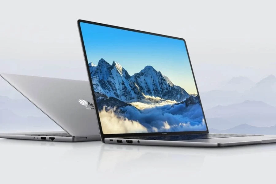
3. The Gram 15 15Z80T includes a 15.6-inch 1080p IPS display with a brightness of 350 nits.
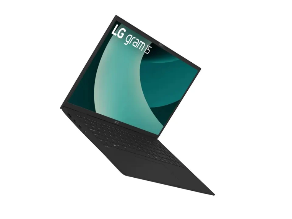
4. Connectivity options for the Gram 15 15Z80T include two USB Type-A, two USB Type-C ports, and a full-sized HDMI port.
5. The Gram 15 15Z80T is lightweight at 1.29 kg and is priced at €1,499 (approximately $1,616) in Europe, with no release date announced for other regions.
LG has refreshed its Gram laptop lineup by introducing a new processor choice, showcasing the Intel Arrow Lake-H and Lunar Lake options that were revealed late last year. These newer models take the place of the Intel Meteor Lake-powered versions, such as the Gram 17 17Z90S (currently priced at $999 on Amazon), which received high praise in our review from last year.
New AMD Options
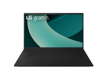
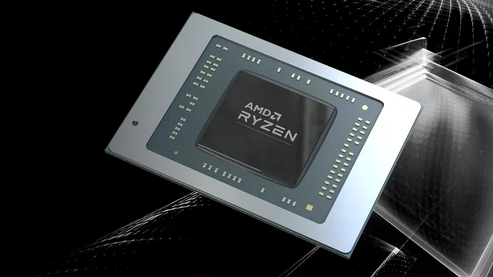
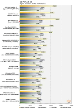
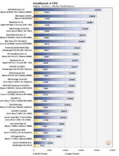
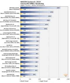
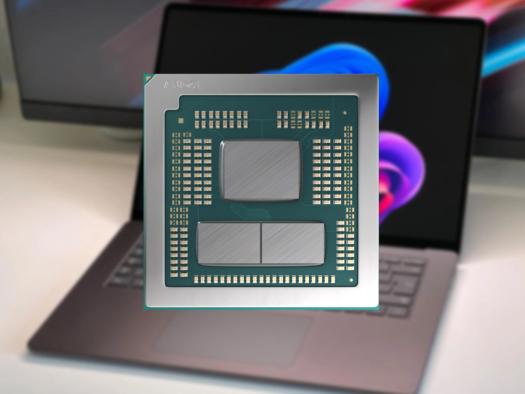
Additionally, LG has broadened its offerings with 15-inch models that utilize AMD’s Krackan Point architecture. The specific model, Gram 15 15Z80T, is equipped with the Ryzen AI 7 350, a chip that performed well in the Vivobook 16 we assessed earlier this year. As we previously mentioned, the Ryzen AI 7 350 is built with four cores each of Zen 5 and Zen 5c CPUs along with a Radeon 860M integrated GPU that features 8 Compute Units (CUs) based on the RDNA 3.5 framework.
Display and Connectivity
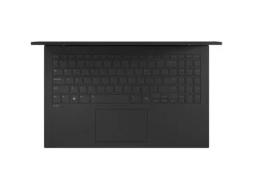
The Gram 15 15Z80T sports a 15.6-inch 1080p IPS display with a 16:9 aspect ratio and offers a peak brightness of only 350 nits. Furthermore, LG has incorporated two USB Type-A and Type-C ports each, in addition to a full-sized HDMI port, all packed into a lightweight design of just 1.29 kg. Currently, the Gram 15 15Z80T is available at various European retailers starting at €1,499 (approximately $1,616), featuring 16 GB of RAM and 1 TB of storage. However, LG has yet to announce when this AMD Krackan Point-powered laptop will be launched in other regions.
Source:
Link
