
ASML (Advanced Semiconductor Materials Lithography) is a Dutch company that specializes in the design and manufacturing of lithography machines for the semiconductor sector. These machines play a crucial role in the chip-making process.
Access to ASML’s state-of-the-art lithography technology has significantly contributed to TSMC’s (Taiwan Semiconductor Manufacturing Company) success as a leading contract chip manufacturer, serving major industry players like NVIDIA and Qualcomm.
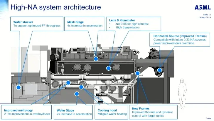
High-NA Lithography Technology
ASML’s latest announcement reveals that it will ship its most advanced lithography machine, valued at US$ 380 million (~2.753 billion yuan), to TSMC within this year. ASML’s Chief Financial Officer, Roger Dassen, disclosed during a recent conference call that both TSMC and Intel, their two biggest clients, will receive the high numerical aperture (high-NA) extreme ultraviolet (EUV) lithography technology by 2024.
ASML has already delivered the world’s first commercial high-NA EUV lithography machine to Intel, with the initial unit being sent to an Oregon factory in late December. The exact timing for TSMC to receive this advanced tool remains unspecified.
The high-NA lithography technology is anticipated to shrink transistor sizes by 66%. This reduction enables chip manufacturers to pack more transistors into the same silicon area, enhancing power efficiency and sustained performance.
Technical Advancements
The high-NA EUV system achieves a numerical aperture of 0.55, improving accuracy and allowing for more intricate silicon patterning compared to previous EUV systems with a 0.33 numerical aperture lens. The new machine is also 30% larger than its predecessors, which already required three Boeing 747s for transportation.
Regarding TSMC, the development of their 2nm nodes is reportedly on track. The company plans to start developing the N3X and N2 processes in Q2 2025, with mass production of N2P and A16 slated for Q2 2026. The 2nm process will incorporate Gate-all-around FETs (GAAFET).
TSMC predicts that its 2nm process will offer a 10% to 15% performance boost and reduce power consumption by 25% to 30%.

Leave a Reply