
According to a recent announcement from South Korean semiconductor manufacturer SK Hynix, the company has introduced a new line of storage products, showcased at the FMS 2024 Summit. This new development features USF 4.1 universal flash memory.
New UFS 4.1 Flash Memories Unveiled
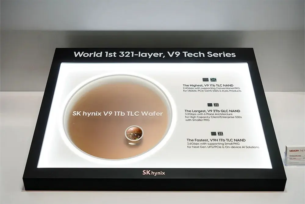
SK Hynix presented two UFS 4.1 universal flash memories with capacities of 512GB and 1TB respectively. These are based on 321-layer stacked V9 1Tb TLC NAND flash memory. In addition to revealing the 1Tb capacity and 2.4Gbps rate TLC, the company also introduced the industry-leading 3.2Gbps V9 2Tb QLC and 3.6Gbps high-speed V9H 1Tb TLC particles for the first time.
Anticipated Improvements in Data Transfer Rates
While detailed specifications of the UFS 4.1 storage chips have not been officially released, it is rumored that UFS 4.1 storage offers a data transfer rate of 8 gigabits per second (GB/s), compared to the 4 GB/s offered by the UFS 4.0 storage chips.
The latest UFS specification available is UFS 4.0, published in August 2022, which specifies a theoretical interface speed of up to 46.4Gbps per device. USF 4.1 is expected to further enhance the transfer rate.
Previous Announcements and Future Expectations
In May this year, the company also revealed its development of the ZUFS 4.0 (Zoned UFS). This NAND flash memory chip enhances data management efficiency and optimizes data transfer between the operating system and storage devices. Applications for this product include various electronic devices such as digital cameras and smartphones. It is also said to improve the performance of on-device AI applications.
UFS 4.1 is anticipated to further boost the storage performance of smartphones and other electronic devices. According to a previous leak, these improvements might be experienced with the Galaxy S25 Ultra.

Leave a Reply