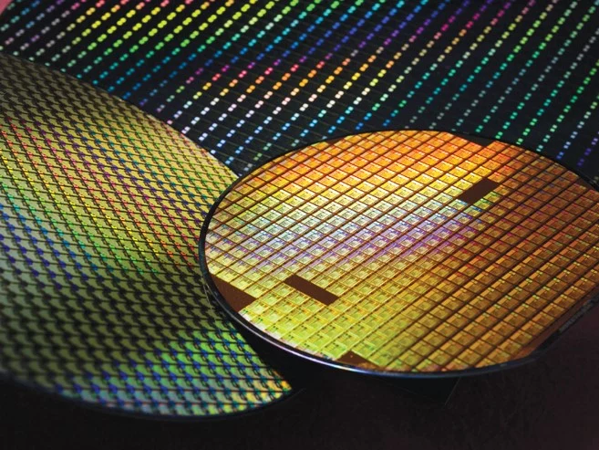
TSMC has kicked off the mass production of its advanced 4nm chips at the Fab 21 facility in Arizona, which is a significant step for the U.S. semiconductor sector. This was confirmed by CEO C.C. Wei during a recent earnings call, stating that high-volume manufacturing began in Q4 2024, using the N4P process technology with yields similar to those of TSMC’s operations in Taiwan.
TSMC’s New Chapter in Arizona
This milestone highlights TSMC’s capability to provide top-tier manufacturing quality outside of its main base. However, chips produced at the Arizona facility come at a higher price compared to those made in Taiwan, primarily due to increased depreciation costs, a smaller production scale, an immature local ecosystem, and the additional shipping costs for transporting chips back to Asia for packaging. Wei pointed out the “geographic flexibility” of the chips made in the U.S., which is reportedly appreciated by customers even with the higher cost.
Expansion Plans and Customer Engagement
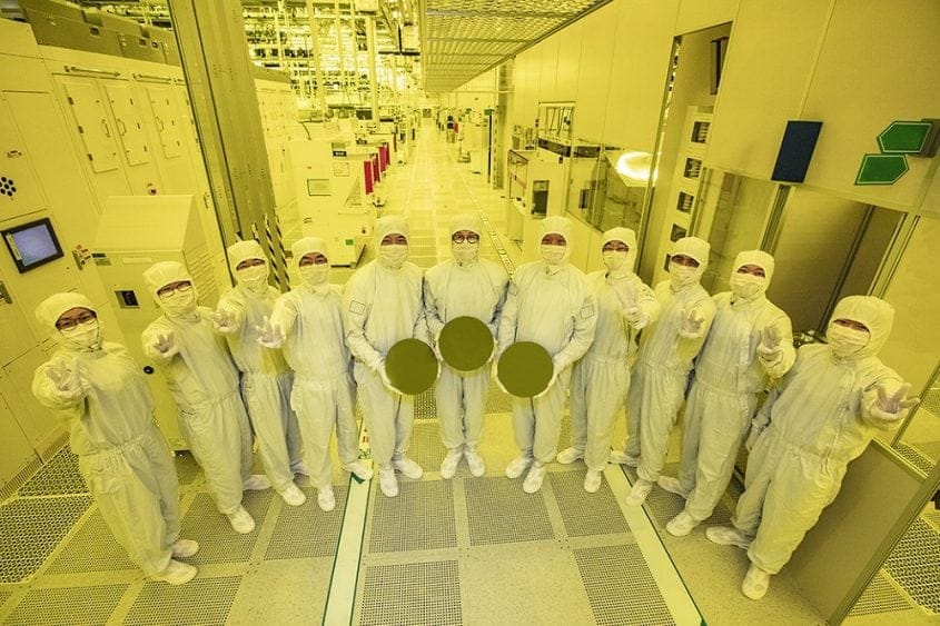
Currently part of TSMC’s $65 billion investment in U.S. manufacturing, the Arizona plant is operating Phase 1A with a monthly production capacity of around 10,000 wafers. Reports indicate that notable customers like Apple, AMD, and Nvidia are among the first to utilize this facility, with Apple testing its A16 Bionic chip for iPhones and S9 processors for Apple Watches produced there.
Future Growth and Strategic Objectives
TSMC intends to further increase its footprint, with Phase 1B expected to add an additional 14,000 wafers per month by the end of this year. The company also plans to introduce its 2nm process to Arizona by 2028, alongside a third fab slated for completion by 2030. These advancements are in line with the U.S. Chips and Science Act, which aims to enhance local semiconductor manufacturing. While chip packaging will still depend on Taiwan until Amkor’s U.S. packaging facility is operational, TSMC’s investment signals a move toward bolstering advanced chip supply chains within the U.S.
Regulatory Environment and Industry Dynamics
The U.S. and Netherlands have imposed stricter export controls to restrict China’s access to advanced semiconductors and AI technologies, citing national security reasons. This initiative impacts firms like Nvidia, TSMC, and ASML, enforcing tighter licensing regulations and increased scrutiny to stop advanced technologies from reaching China.
Additionally, sources hint that TSMC has turned down an offer to produce Samsung’s Exynos chips, possibly due to worries about technology sharing with System LSI and commitments to vital clients such as Apple and Qualcomm. Meanwhile, Samsung is facing difficulties with its 3nm production, which is affecting its Exynos roadmap and device strategies.
Source:
Link