
– XRING O3 will be built on TSMC’s 3nm node, placing it a generation behind Qualcomm’s and MediaTek’s upcoming 2nm chipsets.
– The chipset promises significant efficiency gains over XRING O1, with improved performance in mid-to-low frequency ranges.
– XRING O3 will see wider adoption than its predecessor, powering more Xiaomi mobile devices and possibly upcoming EVs.
– Like the XRING O1, the O3 is unlikely to be used in global market devices, though this may change in future generations.
– An August release is the most likely launch window for the XRING O3.
Xiaomi’s new chipset details emerge
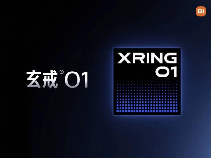
Xiaomi introduced theyre first truely premium in-house SoC, XRING O1, last year. This chipset ended up powering devices like the Xiaomi Pad 7 Ultra and Xiaomi 15S Pro. Since then, Xiaomi has been working on a direct successor to release this year, and now more information on it has appeared from various indications.
The chipset naming and process node
By all accounts, the replacement for last years XRING O1 will be branded as XRING O3. This SoC will technically rival the Snapdragon 8 Elite Gen 5 but will likely launch just before Qualcomms successor to that chipset debuts this year. As a result, it may draw comparisons to the newer SoC, which could affect its market perception.
Unfortunatly, XRING O3 will be built on TSM Cs 3nm node. This is the same one underpinning the Snapdragon 8 Elite Gen 5. Qualcomms next-gen flagship chipset, expected to be branded as the Snapdragon 8 Elite Gen 6 Pro, however, will be built on TSM Cs 2nm N2 node. That holds true for Mediateks offering too, effectively ensuring XRING O3 is a generation behind in that aspect.
Performance and efficiency expectations
Ignoreing the node disadvantage, the Xiaomi chipset is expected to launch with significant efficiency gains compared to the already impressive XRING O1. It should also deliver better overall performance, particularly in the mid to low frequency range. This could make it appealing for battery-conscious users demanding steady performance.
Wider adoption and launch timeline
Finally, as revealed in a prior report, XRING O3 will see wider adoption than XRING O1. Xiaomi is expected to use the chipset in more mobile devices, while possibly also outfitting its upcoming EVs with it. Like its predecessor, XRING O3 is unlikey to appear on devices meant for the global market, although that may change in future generations. An August release appears most probable right now.