
Key Takeaways
1. Prinano has delivered its first PL-SR nanoimprint lithography system, becoming the second company after Canon to place a nanoimprint device with a client for chip production.
2. The PL-SR system supports line widths under ten nanometers but does not guarantee the ability to manufacture advanced logic at the five-nanometer node.
3. Nanoimprint technology reduces energy consumption and equipment costs by avoiding extreme ultraviolet light sources but has trade-offs in throughput and flexibility.
4. The PL-SR system features precise alignment and can handle 300 mm wafers, with a unique template-profile control mechanism to minimize distortion and improve yield.
5. Practical applications for the technology include NAND Flash, silicon microdisplays, silicon photonics, and advanced packaging, helping Chinese manufacturers reduce reliance on foreign tools.
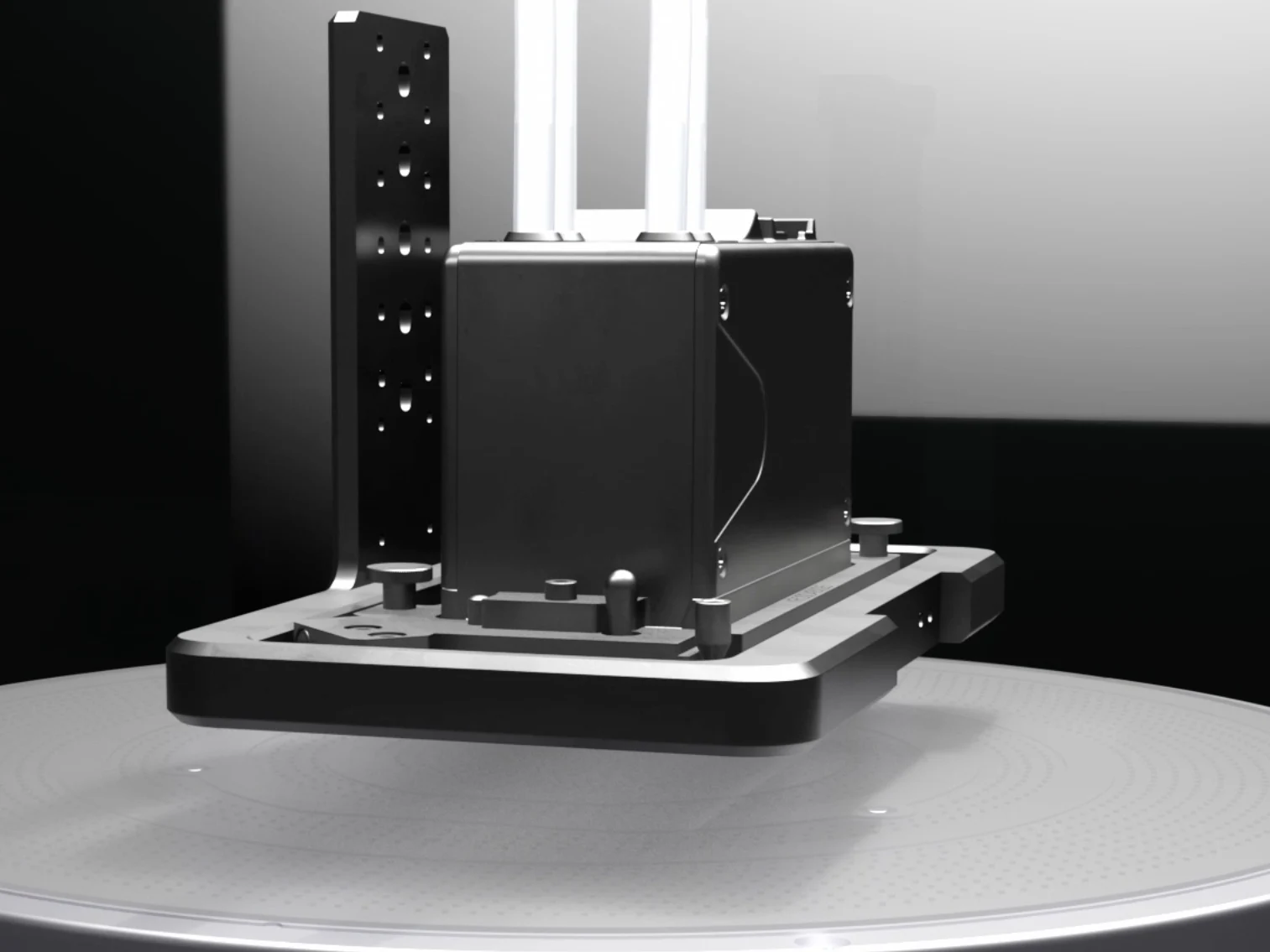
Chinese equipment maker Prinano has recently delivered its first self-designed PL-SR step-and-repeat nanoimprint lithography system to a domestic client that specializes in unique processes. This system is now ready for actual chip production following testing by the customer, making Prinano just the second company, alongside Canon, to successfully place a nanoimprint device with a client.
Specifications and Performance
The PL-SR system is capable of supporting line widths that are less than ten nanometers. In comparison, Canon’s FPA-1200NZ2C achieves a line width of approximately fourteen nanometers. While it is marketed as being suitable for producing five-nanometer-class chips, it should be noted that the documents indicate Prinano’s device does not necessarily mean the PL-SR can manufacture advanced logic at a five-nanometer node.
Advantages and Trade-offs
The attraction of nanoimprint technology is quite clear: it bypasses the extreme ultraviolet light sources that are typically used in commercial EUV lithography, which helps to reduce both energy consumption and equipment costs. However, this comes with trade-offs in terms of throughput and flexibility, as nanoimprint technology is generally slower than traditional optical lithography and is not ideal for complex logic processes that require intricate, advanced patterns.
Prinano’s machine operates by pressing a rigid quartz mold, which is engraved with nanoscale circuitry, into a thin resist layer that has been deposited using inkjet technology. The inkjet module of the system smartly controls droplet volume to maintain a thin residual layer (under ten nanometers with less than two nanometers variation) before curing the pattern for the next etching process. The tool can handle 300 mm wafers, aligns the mold and wafer with precise tolerances, and sequentially imprints each field with stitching to cover the entire wafer. It also allows for uniform template joins ranging from 20 mm x 20 mm to 300 mm x 300 mm.
Practical Applications
A unique template-profile control mechanism is designed to address curvature mismatches between the mold and wafer, allowing for the transfer of features with aspect ratios exceeding seven-to-one while minimizing distortion. This is crucial for improving yield and reducing device variability. After the imprinting process, the resist acts as a mask for etching the final structures.
The initial validation phase is aimed at applications that require regular, repetitive patterns, such as NAND Flash, silicon-based microdisplays, silicon photonics, and advanced packaging. These areas can take advantage of the technology’s fine pitch and field-by-field stitching, without requiring the pattern diversity often needed by CPUs and GPUs. Furthermore, this development positions domestic nanoimprint technology as a means for Chinese memory manufacturers to lessen their reliance on foreign tools and compete more effectively with established suppliers.
Source:
Link
Leave a Reply