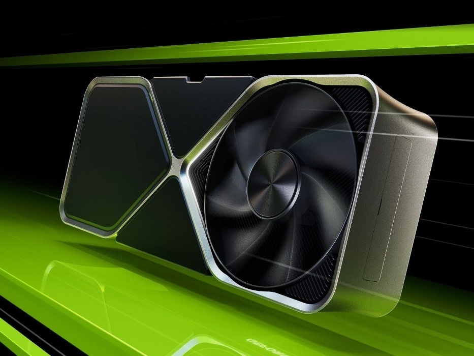
Just a day after the PCB for the eagerly awaited GeForce RTX 5090 was leaked, the same source has now shared an image of the GPU itself. This picture showcases the GB202, a graphics processor based on the Blackwell architecture, which is set to be the heart of the RTX 5090. The official reveal is anticipated to take place in early January at CES 2025.
Specifications of the RTX 5090
At the core of the RTX 5090 is the GB202-300 silicon, marking it as the largest gaming GPU in NVIDIA’s Blackwell series with a remarkable 21,760 CUDA cores. The physical size of the GB202 is considerable, measuring around 63 × 56 mm. The die itself occupies a substantial area of 24 × 21 mm, leading to an overall die size of 744 mm².
Memory and Performance
Surrounding the GPU are 16 Samsung GDDR7 memory chips, contributing to a total memory capacity of 32 GB. The combination of numerous chips, the large GPU package, and a high pin count strongly suggests a 512-bit wide memory bus. If the memory speed reaches 28 Gbps, this setup could achieve an astonishing memory bandwidth of 1,792 GB/s, representing a major advancement compared to earlier models.
Power and Launch Details
To power this powerful GPU, a sturdy 24-phase VRM solution is implemented. It is anticipated that the card will utilize a single 12+4-pin 12V-2×6 power connector. Given that this connector can handle 600W of continuous power, experts in the industry predict that the Total Graphics Power (TGP) for the RTX 5090 could be between 500 and 550W, or maybe even more.
Both the GeForce RTX 5090 and RTX 5080 are set to debut in January at CES 2025, with the RTX 5080 possibly arriving on the market ahead of its more advanced counterpart. The existence of samples with board partners, along with the matching NVIDIA branding on the GPU label, further confirms the credibility of these leaks. The only detail still unknown is when production of the GPU will actually begin.
Source: Link


Leave a Reply