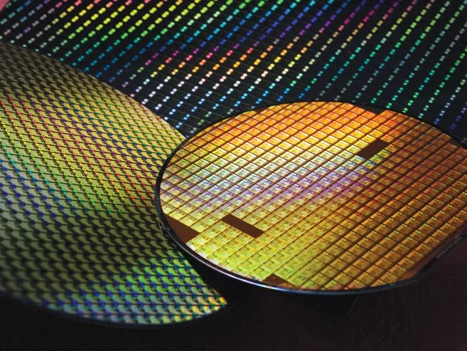
Tag: TSMC N2

  • iPhone 18 Pro and Fold to Boost Performance with 2nm A20 SoC

    iPhone 18 Pro and Fold to Boost Performance with 2nm A20 SoC

    Key Takeaways

    1. The iPhone 17 Pro and Pro Max will feature the Apple A19 chip, while the Apple A20 is expected to use TSMC’s new 2-nanometer N2 process.
    2. The A20 chip could offer a 15% power increase and a 30% efficiency improvement, even without architectural upgrades.
    3. The Apple A20 may utilize advanced Wafer-Level Multi-Chip Module packaging, integrating memory directly onto the chip.
    4. This new design could enhance memory bandwidth, reduce power use, and save space for potentially larger batteries.
    5. The A20 chip is anticipated to debut in the iPhone 18 series, with possible delays if TSMC’s production timeline is not met.


    While the next iPhone 17 Pro and iPhone 17 Pro Max are anticipated to come with the Apple A19 chip, which is likely to be produced using TSMC’s N3P process, analyst Jeff Pu now claims that the Apple A20 will be produced using a new 2-nanometer technology, specifically TSMC’s N2 process. This advancement could enhance the chipset’s power by up to 15% and improve its efficiency by 30%, even disregarding any possible architectural upgrades.

    Notable Packaging Innovations

    Another key enhancement for the Apple A20 could be the advanced Wafer-Level Multi-Chip Module (WMCM) packaging process. In simple terms, this means that the memory will be integrated directly onto the chip instead of relying on separate RAM modules on the mainboard. Although this design is pricier, it has the potential to deliver much higher memory bandwidth and a slight reduction in power use. Jeff Pu mentions that this method could also save some space on the mainboard, potentially allowing Apple to include a slightly larger battery.

    Future iPhone Models

    Regardless, the Apple A20 SoC is set to make its first appearance in the iPhone 18 Pro, iPhone 18 Pro Max, and iPhone 18 Fold, which are expected to be announced in September 2026. As is common with early speculation, these details and assertions should be viewed skeptically. Apple’s plans could shift if TSMC fails to meet its production timeline for the N2 process. Furthermore, the base versions of Apple’s forthcoming smartphones are likely to feature last-generation chips to maintain more affordable pricing.

    Source:
    Link

  • MediaTek Develops Next-Gen 2nm Chip Technology

    MediaTek Develops Next-Gen 2nm Chip Technology

    Key Takeaways

    1. Attention is shifting from 3 nm to upcoming 2 nm mobile SoCs, with uncertainty around Apple’s adoption of TSMC’s N2 node.
    2. MediaTek plans to tape-out its 2 nm product, likely the Dimensity 9600, in September 2025, aiming for market release by the end of 2026.
    3. High-volume production of TSMC’s N2 process is expected to start in the latter half of 2026.
    4. MediaTek’s Dimensity 9600 may change the trend of being cheaper than Qualcomm’s chips, especially with rising costs of N2 wafers.
    5. Detailed specifications for the Dimensity 9600 are not yet available, as the chip is still over a year away from release.


    Now that 3 nm mobile SoCs have been in the market for some time, attention is shifting towards the next major transition: 2 nm. Apple typically leads the way in adopting new technologies, but it’s unclear whether they will embrace TSMC’s N2 node. If Apple ends up sticking with the N3P process, MediaTek could potentially be the first to launch a 2 nm smartphone SoC.

    MediaTek’s Timeline

    During its Computex 2025 presentation, the Taiwanese semiconductor company announced that its 2 nm product is set to tape-out in September 2025. This means the design will be completed before it begins mass production. A previous list from TSMC indicated that MediaTek is one of the customers for the 2 nm technology. High-volume production for the N2 process is expected to kick off in the latter half of 2026, and if everything goes as planned, MediaTek’s smartphone SoC could hit the market by the end of 2026.

    The Dimensity 9600

    The chip in question is likely the Dimensity 9600. However, no details about this SoC have emerged yet, and it may take a while for that to happen since the chip is still more than a year away from its release. In the past, MediaTek’s chips were generally cheaper than those of Qualcomm, but this trend might change with the Dimensity 9600. TSMC’s N2 wafers are already quite expensive, and they could become even costlier if the anticipated 10% price increase is implemented.


  • TSMC 2nm Wafers Expected to See 10% Price Increase

    TSMC 2nm Wafers Expected to See 10% Price Increase

    Key Takeaways

    1. TSMC’s N2 node is in high demand from major companies like AMD, Nvidia, Apple, and Qualcomm, leading to higher pricing for wafers.
    2. Wafer prices are expected to rise further due to construction costs of fabs, economic uncertainty, and TSMC’s need to recover significant investments.
    3. The cost of TSMC’s 2 nm wafers is projected to increase by 10%, potentially reaching around $33,000 for a 300 mm wafer.
    4. Smaller OEMs might shift to older nodes (N3, N4) or consider Samsung Foundry’s 2 nm options due to rising TSMC prices.
    5. Intel’s innovative 18A and 14A nodes are becoming competitive alternatives, featuring technologies not available from TSMC and Samsung Foundry for several years.


    With the increasing demand from companies like AMD, Nvidia, Apple, Qualcomm, and even Intel, which has its own fabrication plants, TSMC’s N2 node is becoming one of the most wanted in recent times. This high demand allows the Taiwanese semiconductor manufacturer to set higher prices.

    Rising Wafer Prices

    A new report from Ctee suggests that wafer prices might rise even further in the upcoming weeks. Insiders believe this is due to the increasing expenses of constructing fabs in countries like the United States, the overall uncertainty in the global economy, and the need to recover some of the $38-42 billion that TSMC intends to invest this year for capital projects.

    Cost of TSMC’s 2 nm Wafers

    A wafer at TSMC’s 2 nm node is expected to be 10% pricier than previously. Last year, the estimated cost was around $30,000 for a 300 mm wafer, which means the new price could reach about $33,000. The report mentions that Nvidia’s CEO, Jensen Huang, finds TSMC’s advanced nodes to be “very worth it.”

    Nvidia plans to use the N2 node for its upcoming Rubin Next architecture. It will also be utilized in AMD’s Zen 6 processors, Apple’s A21 and M5 chips, MediaTek’s Dimensity SoC, and potentially even in the CPU tile of Intel’s Nova Lake desktop series.

    Smaller OEMs and Alternatives

    This situation might lead many smaller OEMs to consider older options like the N3 and N4 nodes. Alternatively, they may explore Samsung Foundry’s 2 nm offerings (SF2/SF2P), which Qualcomm is reportedly looking into. If TSMC’s wafer prices continue to escalate, Samsung Foundry could have a genuine opportunity for a resurgence, assuming they can stabilize their yields.

    Intel’s 18A and 14A nodes are also becoming strong contenders due to their innovative technology like backside power delivery, which TSMC and Samsung Foundry won’t have access to for a few more years.

    Source:
    Link