Key Takeaways
1. The Nintendo Switch 2 has officially launched, with a new price list for repairs released by Nintendo Japan.
2. Repair costs have significantly increased, with mainboard replacement costing 27,500 yen (around $191), a 92% rise from the original Switch.
3. The cost for replacing the 8-inch display is 15,400 yen (about $115), which is 27% higher than the Nintendo Switch OLED and 55% more than the original.
4. Battery replacements are priced at 9,900 yen (about $69), reflecting a 63% increase, despite similar capacity to previous models.
5. Repairing a Joy-Con costs 3,960 yen (around $28), a 38% increase from the first generation, while dock repairs are priced at 6,930 yen (approximately $48), over double the previous model’s cost.
The Nintendo Switch 2 is now officially released. As part of the launch, Nintendo Japan has shared a price list detailing the repair costs for the new console. Since repairs at Nintendo are typically pricier in Japan, customers in other countries might face even steeper charges.
Rising Repair Costs
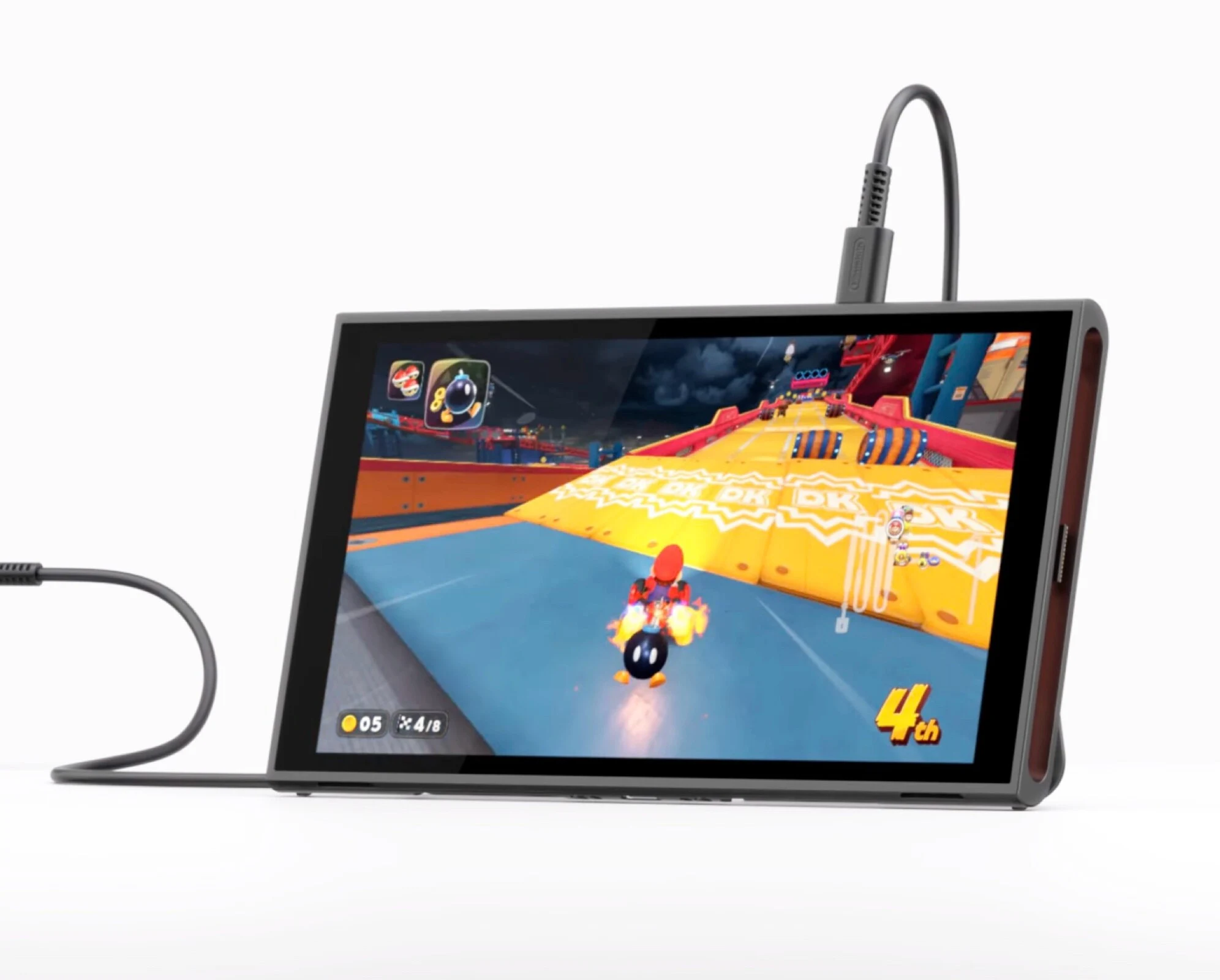
The price list reveals a significant increase in repair expenses. For instance, replacing the mainboard with the upgraded Nvidia Tegra T239, which features 12 GB of RAM and 256 GB of flash storage, will set you back 27,500 yen (around $191). This is a staggering 92% increase compared to the original Nintendo Switch. Meanwhile, the 8-inch, 120 Hz IPS display with a resolution of 1,080p will cost 15,400 yen (approximately $115), which is 27% higher than the Nintendo Switch OLED and 55% more than the original model.
Battery and Component Costs
For a battery replacement, Nintendo is charging 9,900 yen (about $69), which is a 63% increase from previous models, despite the battery maintaining a similar capacity. Some components, like the SD card reader, speakers, and headphone jack, have slightly lower repair costs, priced at 7,150 yen (roughly $50).
Joy-Con and Dock Repairs
Repairing a faulty dock is priced at 6,930 yen (approximately $48), which is over double the cost of the earlier model. If you need to fix a Joy-Con 2, Nintendo charges a flat fee of 3,960 yen (around $28) for each Joy-Con sent in, which is 38% more expensive than the first-generation Joy-Con. Despite these increases, Nintendo still provides clear flat-rate prices, allowing customers to estimate the costs before sending in their consoles or parts.
Nintendo Japan | Nintendo Germany
Source:
Link


