Tag: Semiconductor Technology

  • Samsung to Mass-Produce 2nm Chips with GAA Technology in 2025

    Samsung to Mass-Produce 2nm Chips with GAA Technology in 2025

    Samsung's semiconductor foundry division has encountered challenges in attracting clients for its latest chip manufacturing technologies, particularly the 3nm and 4nm processes. Despite these hurdles, Samsung remains committed to advancing its technology, with plans to introduce the 2nm process.

    Advancements in Chip Manufacturing

    Samsung is set to commence mass production of chips utilizing the 3nm technology later this year. The upcoming 2nm process will integrate state-of-the-art gate-around transistor (GAA) technology, slated for mass production by 2025. Samsung intends to unveil this cutting-edge technology at forthcoming industry events.

    Gate-Around Transistor Technology

    The GAA technology represents a novel transistor design that enhances efficiency and performance by facilitating improved current flow. Initially incorporated in Samsung's 3nm process, GAA technology has only been utilized in their Exynos processors to date. The first-generation 3nm GAA chip surpasses 5nm chips in terms of area reduction, performance, and energy efficiency.

    Future Prospects

    Samsung aims to scale up chip production using the second-generation 3nm GAA technology by 2024, anticipating even more significant advancements. While rivals like TSMC have yet to adopt GAA technology, both Samsung and TSMC, as well as Intel, are expected to integrate it into their upcoming 2nm processes.

  • Samsung Explores MUF Technology for Next-Gen Server DRAM

    Samsung Explores MUF Technology for Next-Gen Server DRAM

    Samsung is looking into incorporating molded-in-fill (MUF) technology in its next generation of dynamic random-access memory (DRAM), as per a report from TheElec. This decision indicates Samsung's exploration of innovative methods to boost the performance and efficiency of its memory products. The MUF technology, previously employed by SK Hynix in the production of high-bandwidth memory (HBM), presents promising opportunities for Samsung's future DRAM projects.

    Samsung’s tests on an MR MUF process have indicated promising outcomes
    MUF technology involves injecting a substance between semiconductors after creating numerous small holes in the semiconductor layers. This process is designed to securely link multiple vertically stacked semiconductors. Samsung's recent experiments with an MR MUF process for 3D stacked memory have demonstrated improved throughput in comparison to traditional methods like thermal pressed non-conductive film (TC NCF). However, there are concerns about its impact on physical properties.

    Samsung's Strategic Application of MUF Technology

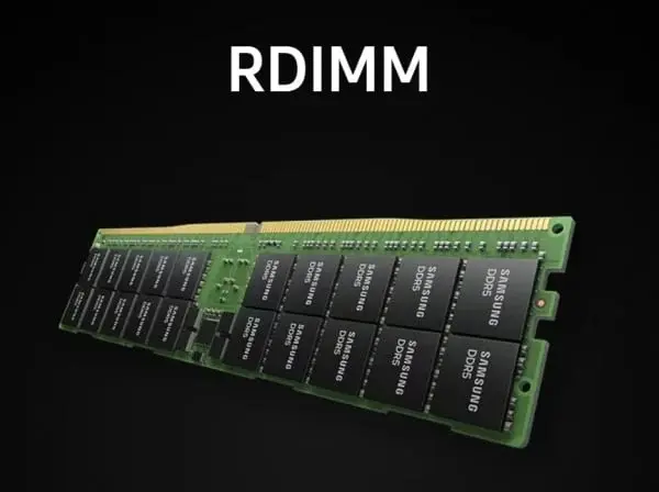
    While Samsung identified MUF as unsuitable for HBM technology due to specific demands, it envisions potential uses in 3DS registered dual in-line memory modules (RDIMMs), predominantly deployed in server settings. This choice is in line with Samsung's dedication to advancing server DRAM memory technologies to meet the changing demands of the industry.

    Advantages of MUF Technology in Semiconductor Industry

    MUF's success in HBM production by SK Hynix has attracted attention in the semiconductor sector. This epoxy resin molding compound is believed to offer benefits such as preventing wafer warpage and enhancing overall performance. Samsung's efforts to develop its proprietary MUF compound in partnership with Samsung SDI indicate a strategic step towards establishing custom solutions tailored to its needs.

    Implications of Samsung's Potential Adoption of MUF Technology

    The potential integration of MUF technology by Samsung carries weight in the semiconductor market. As the world's leading storage semiconductor enterprise, Samsung's backing of MUF could accelerate its broad acceptance and adoption as a mainstream technology. This advancement has the potential to reshape the landscape of the semiconductor material market, ushering in significant changes in the industry.